Faraday Cup design


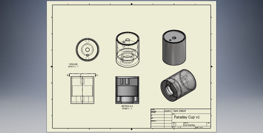
Cup Drawing

CAD (autodesk) files: Faraday Cup

Bias schematic: Diagram

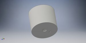
A Faraday cup is an instrument that can be used to measure ion beam currents. I designed this one for testing the anode layer ion source from rtftechnologies.org. It has 2 permanent magnet rods (3/16″ dia x .5″) in the first part of the cup to act as a trap for incoming electrons and the cup can be positively  biased to suppress secondary electrons so that the measured current is just the ion beam.

Between the section with the magnets and the collector, there is an interchangeable aperture so you can use different sizes. This was designed to be hand made on a lathe; there is no tolerancing so do not attempt to make it unmodified on a CNC.  The body, aperture, and collector are made from stainless steel and the ring which holds the magnets and insulates the collector from the body is plastic (ideally PEEK). The backside of the cup has two blind holes, the center for mounting and the offset hole for BNC connection.


Anode Layer Ion Source (RTFtechnologies)

ALIS acquired from Andrew (http://rtftechnologies.org). CF flange, MHV feedthrough, and HV PSU are on order.

Ion source links: http://wiki.zeloof.xyz/index.php/Ion_Source

Abstract: Anode layer ion sources are one type of gridless (no acceleration or focusing grids/screens) closed-drift (electron and plasma movement is confined due to E x B force) ion sources and are therefore a simple way to make a confined ion/plasma stream. These sources commonly operate under partial vacuum in O2/N2/Ar environments. They have many applications, one of which is a high power directional plasma cleaning source which has many advantages over glow discharge or inductively/capacitively coupled plasmas. Their cylindrical geometry can be explained because it allows the E x B currents to converge and close in on themselves rather than being swept to one side in non-cylindrical designs. They are similar to inverted magnetrons and end-Hall ion thrusters in construction and in operation except they often do not require external neutralization for the ion beam.

Neutralizing electrons come from the from the surroundings and collisions of ions with the discharge channel walls because the anode is held at a higher potential than that of a hall effect source and they therefore operate in the self-sustained discharge area. Thus, some of the electrons from the cathode escape into the ion beam and neutralize the space charge on the ions. The extent of space charge neutralization can be related to the electric field strength and therefore the voltage applied to anode. These high voltages are typically in the 800v-2000v range and ALIS devices can operate up into the tens of millitorr down to the 1e-5 torr range at higher voltages.  Continue reading Anode Layer Ion Source (RTFtechnologies)

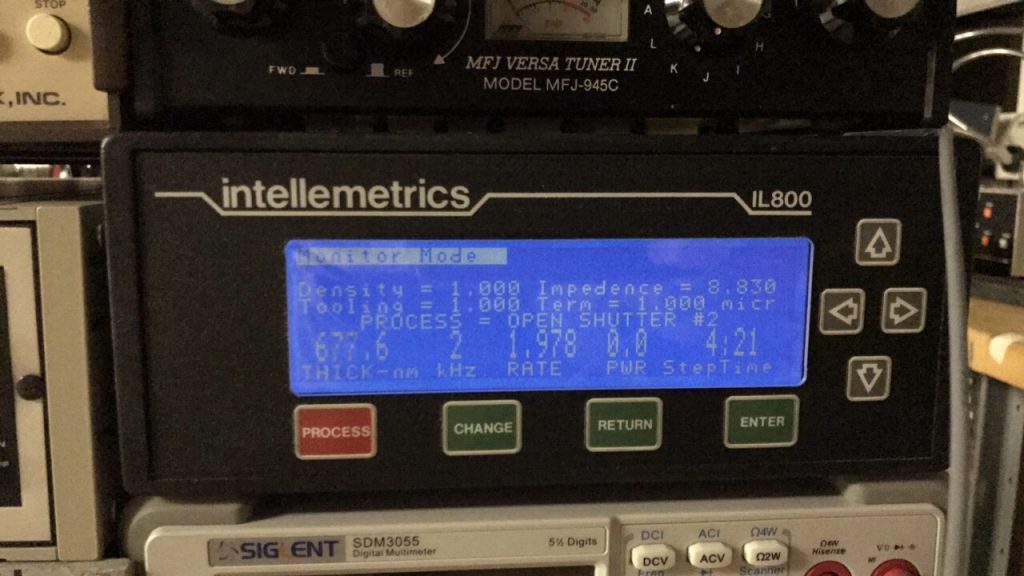
6mhz TTL Oscillator Used as Quartz Microbalance


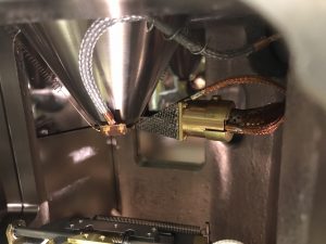
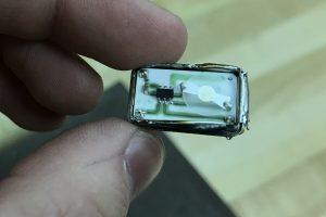
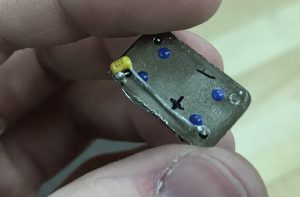
A 6mhz oscillator can was cut up with pliers and the top was removed to expose the quartz crystal. The output is AC coupled (high pass filtered) to the positive (+5v) rail so that a single coax cable can be used to connect this to the thickness monitor as the power is basically just a DC offset on the signal. If you buy a pack of crystals from somewhere like Lesker they will (depending on your thickness monitor) most likely require the usage of an external oscillator. Such a circuit can be made by a complimentary pair or NPN and PNP transistors and couple passive components. Thanks to Ben from Applied Science for the idea.

Abstract: The quartz microbalance is a quick way of monitoring thin film thicknesses in real time, a bare quartz crystal which oscillates at a known frequency is placed in the chamber near the substrate involved in deposition. As the film accumulates on the crystal, it gains mass and the resonant frequency is lowered. The cumulative frequency change is analyzed and interpreted as the rate of accumulation the rate is integrated into a total thickness. Note that accumulation rate is the proper term for deposition rate, as in many cases (sputtering) the actual deposition rate is higher but some atoms are resputtered off the substrate due to high energy molecules in the chamber, substrate temperature, etc. and the total film thickness can momentarily decrease. The net result of the deposition and resputtering is known as accumulation

FullSizeRender

+/- 0.1nm resolution!

Custom Flange Block Off Plate Installation

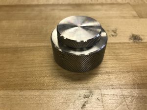
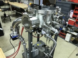
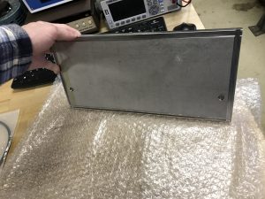
My vacuum chamber which I am setting up for thermal evaporation has a large rectangular flange which has grooves for ISO style clamps and 2 locator pins. This flange may have been used for something like a load lock but as far as I could tell it is not a standard size so a custom block off plate was designed and machined from SS with grooves on the back for clamps, 2 pressed locator pins, and a viton o-ring. Mating surface was hand lapped to ensure good vacuum seal. Made by the extremely talented J.D Guerard machining company.