
(Click on image to enlarge)
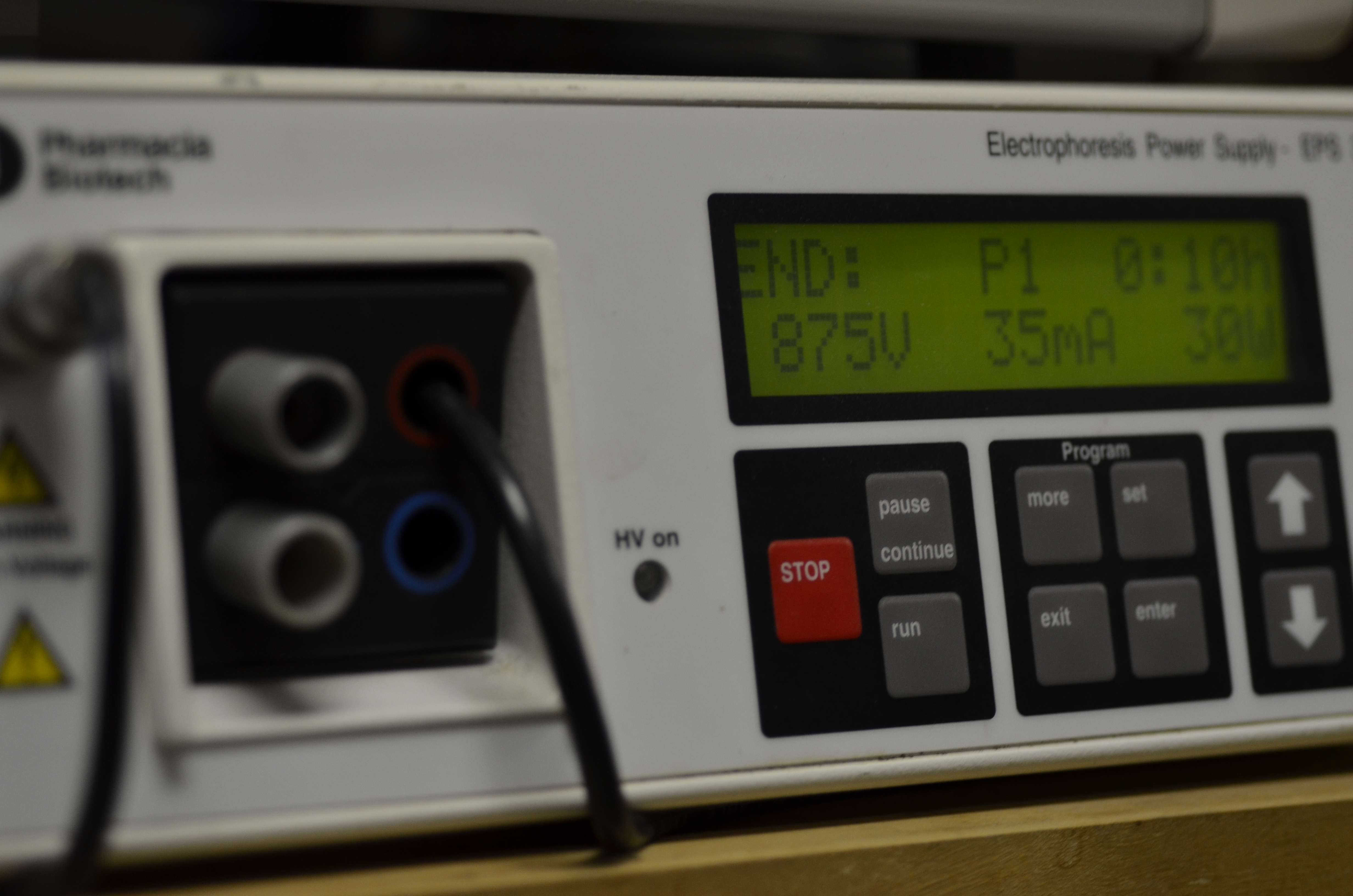
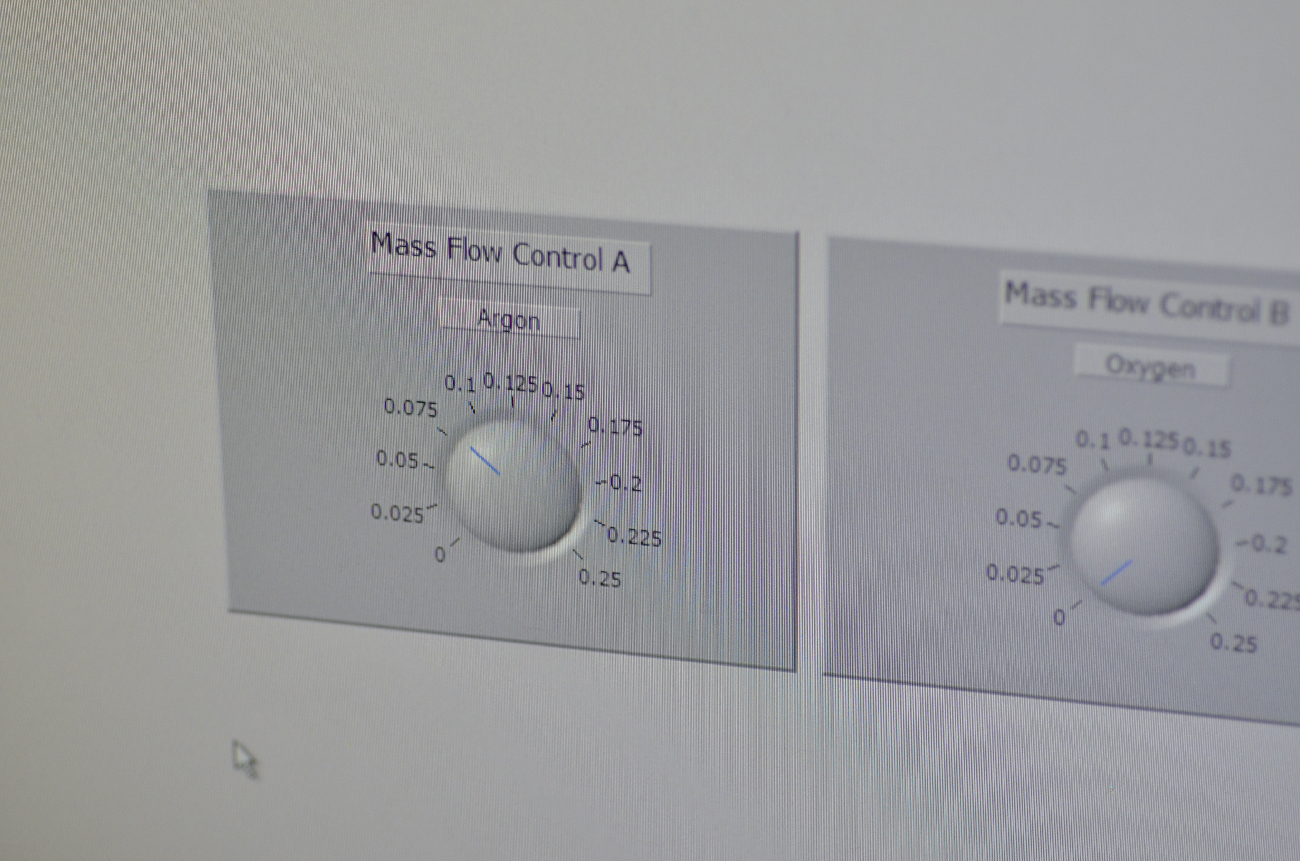
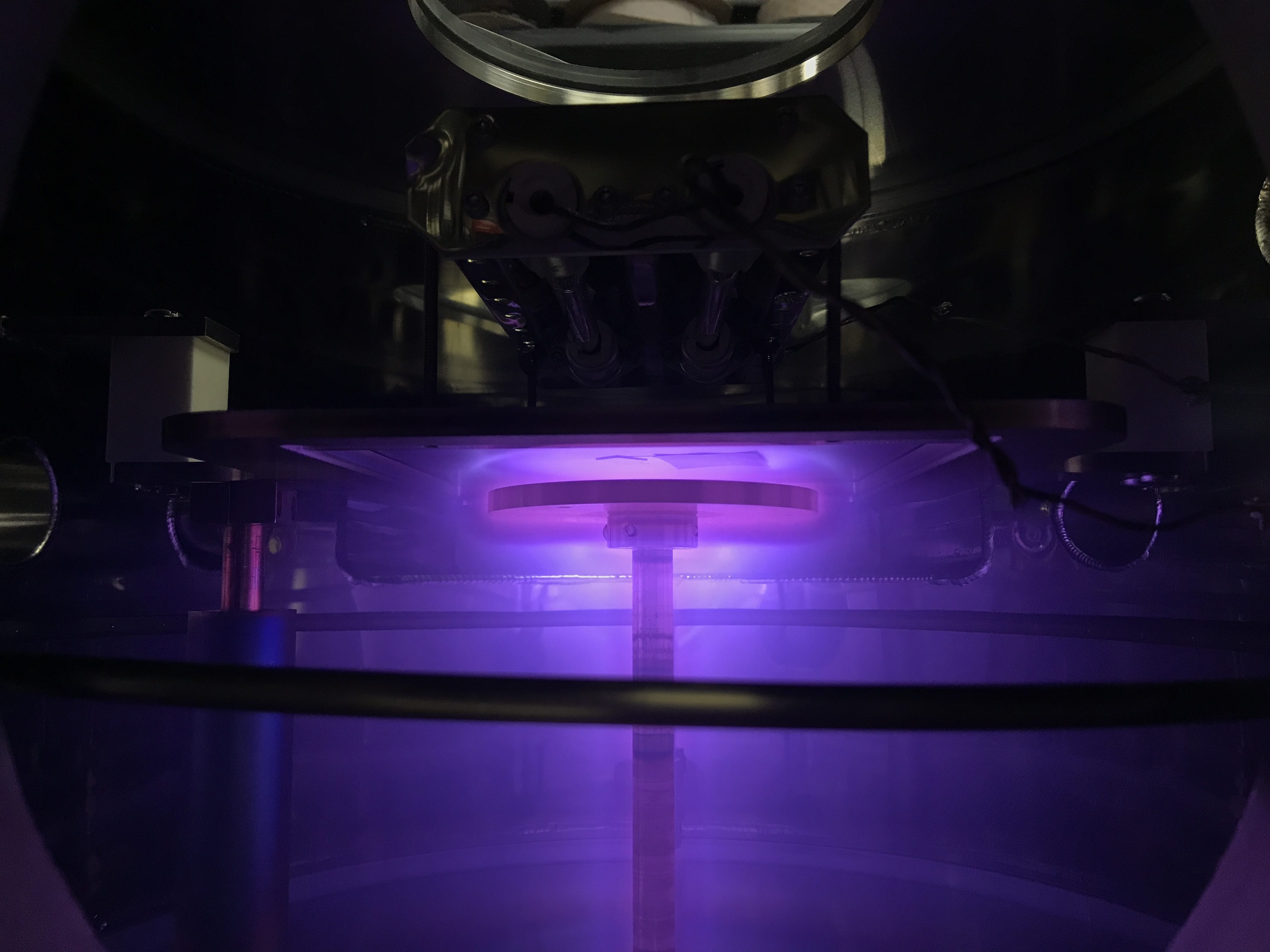
Progress in developing the metalization process for the home chip lab. DC and RF sputtering is used and the process will be refined more and then I will move on to the wet process with etching metal through resist mask, etc.


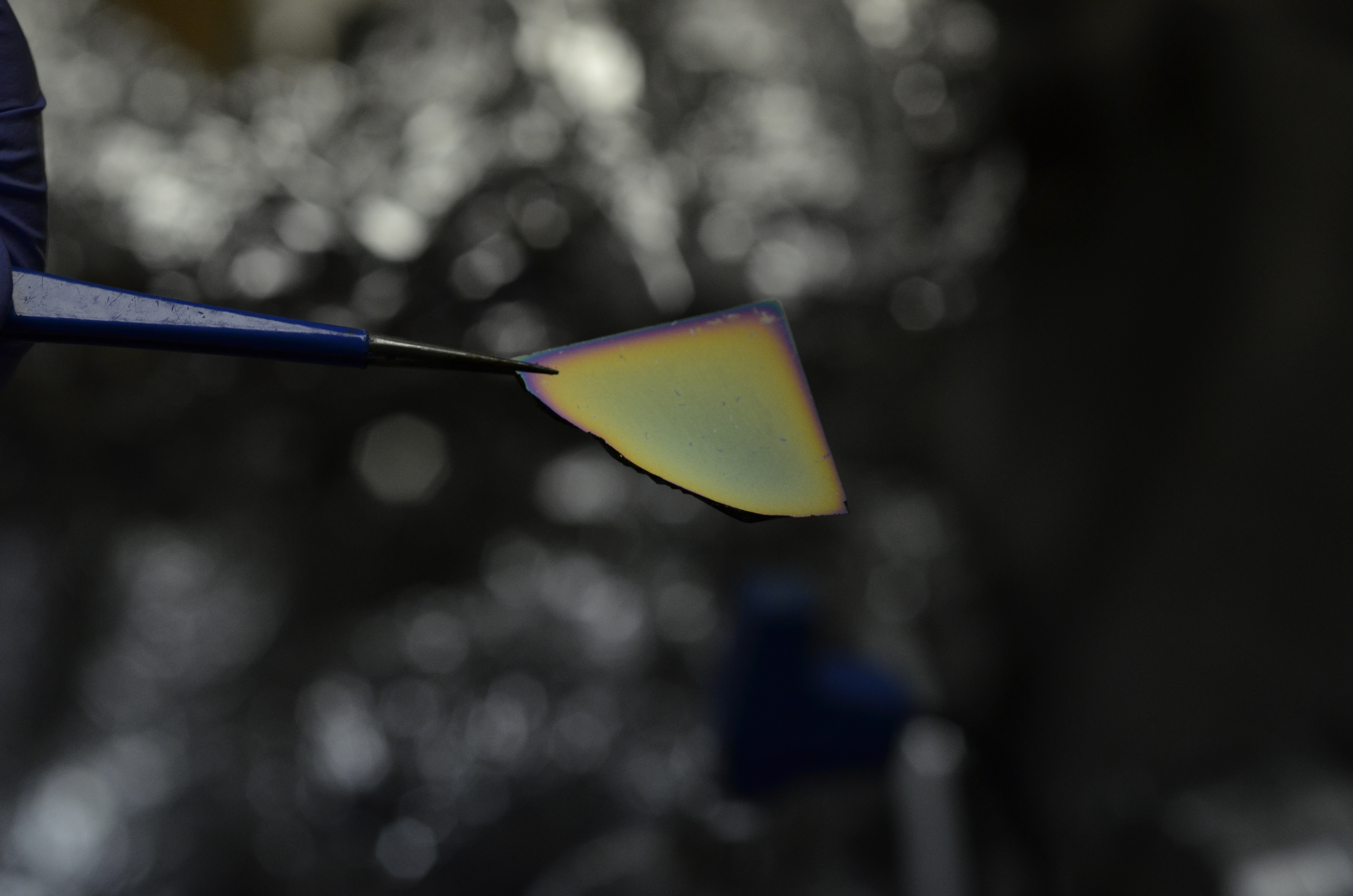
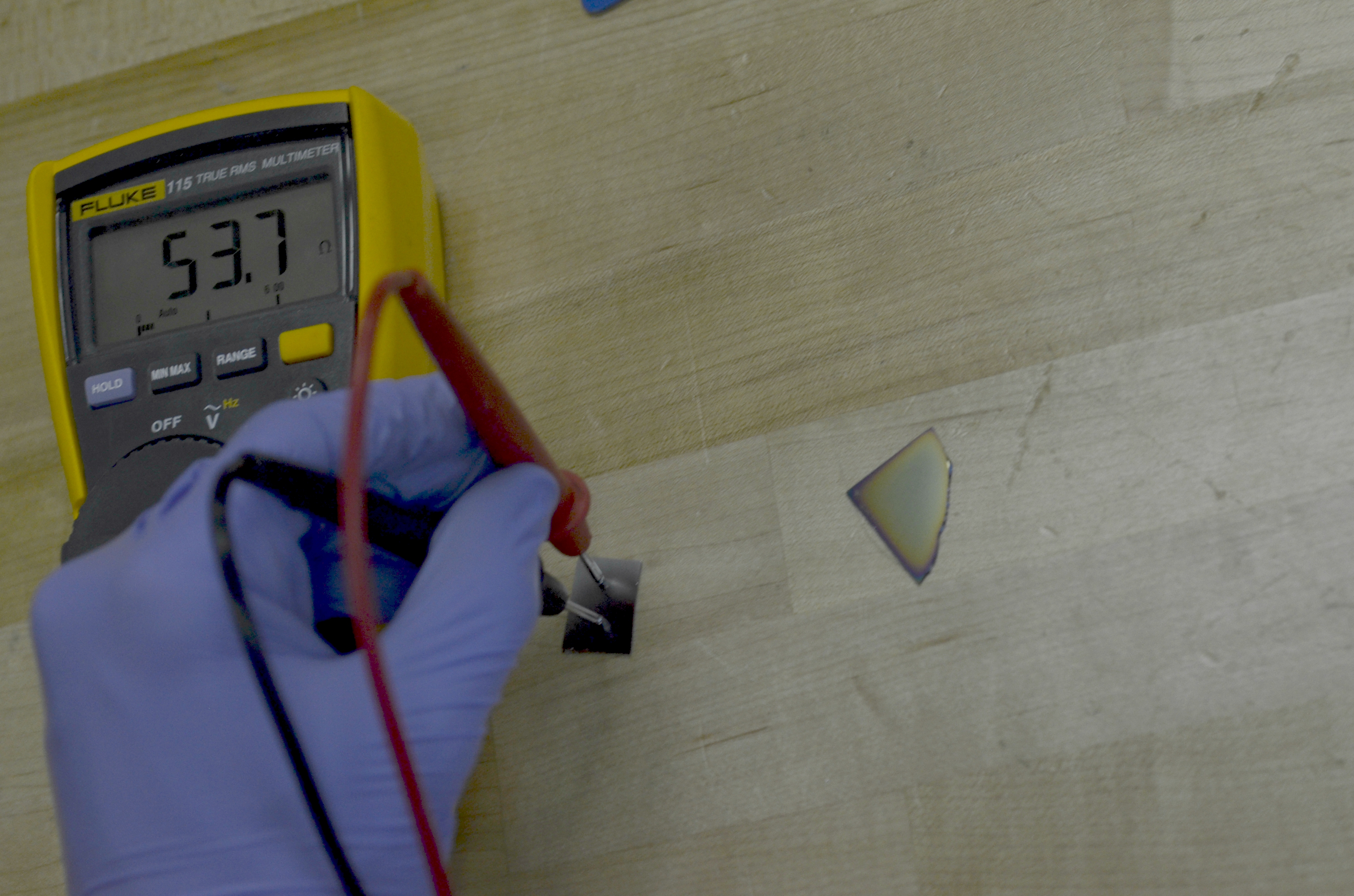
Sample is scratched with a razor and surface roughness is measured with a KLA Tencor Stylus Profiler. Surface is extremely rough and best interpretation of the data leads me to believe the thickness of the sputtered film is approximately 0.492um.
One thought on “Developing Metalization Process for Homemade Microelectronics”