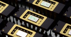
Using a 50W Ytterbium fiber laser to scribe and cut Silicon wafers. Laser wavelength is 1062nm and since Silicon has poor transmission at this low IR wavelength, enough energy is absorbed to make laser marks.
Scribe marks are made at higher speed and must follow perpendicular or parallel to a flat of the <100> wafer so that the scribe lies along a crystal lattice line. When cutting all the way through the wafer, higher power is used and arbitrary shapes that do not follow the crystal lines are possible.


Hello Sam, I wonder how much your investment for the Lab ? I see you use many equipment . How many chip you can produce in 1 month ? I just want to know, is home chip lab can produce commercial chip , monthly quantity ? Thanks