RF or DC oxygen plasmas are composed of a number of highly energetic and reactive species that will readily clean most organics off wafers and strip photoresist.
While operating with prolonged high power plasmas residual gas deposition and chamber sputtering collects on most surfaces.
Field oxide growth – 1200 c w/ water vapor, 5000A blue film
If wafer in storage, dehydration bake – 10 min @ 220c
Check wafer hydrophobic if necessary
Optional spin HMDS
Spin 3.5mL AZ 4210 resist 30 sec @ 3500 rpm ~3.5um film
Soft bake resist 2 min @ 105c hotplate
Expose active area
Develop 1:3 400k KOH:H20 puddle 1 min
Water rinse (no solvent)
Inspect wafer, if defect strip resist and retry
Hard bake 15 min @ 125c hotplate
Etch active area – 1-2% HF 15 min or until surface hydrophobic
Water rinse
Resist strip – Acetone or plasma ashing 100 watts RF 5 min @ 125mTorr O2
IPA rinse
Water rinse
Active area etch
Particles shorting gate
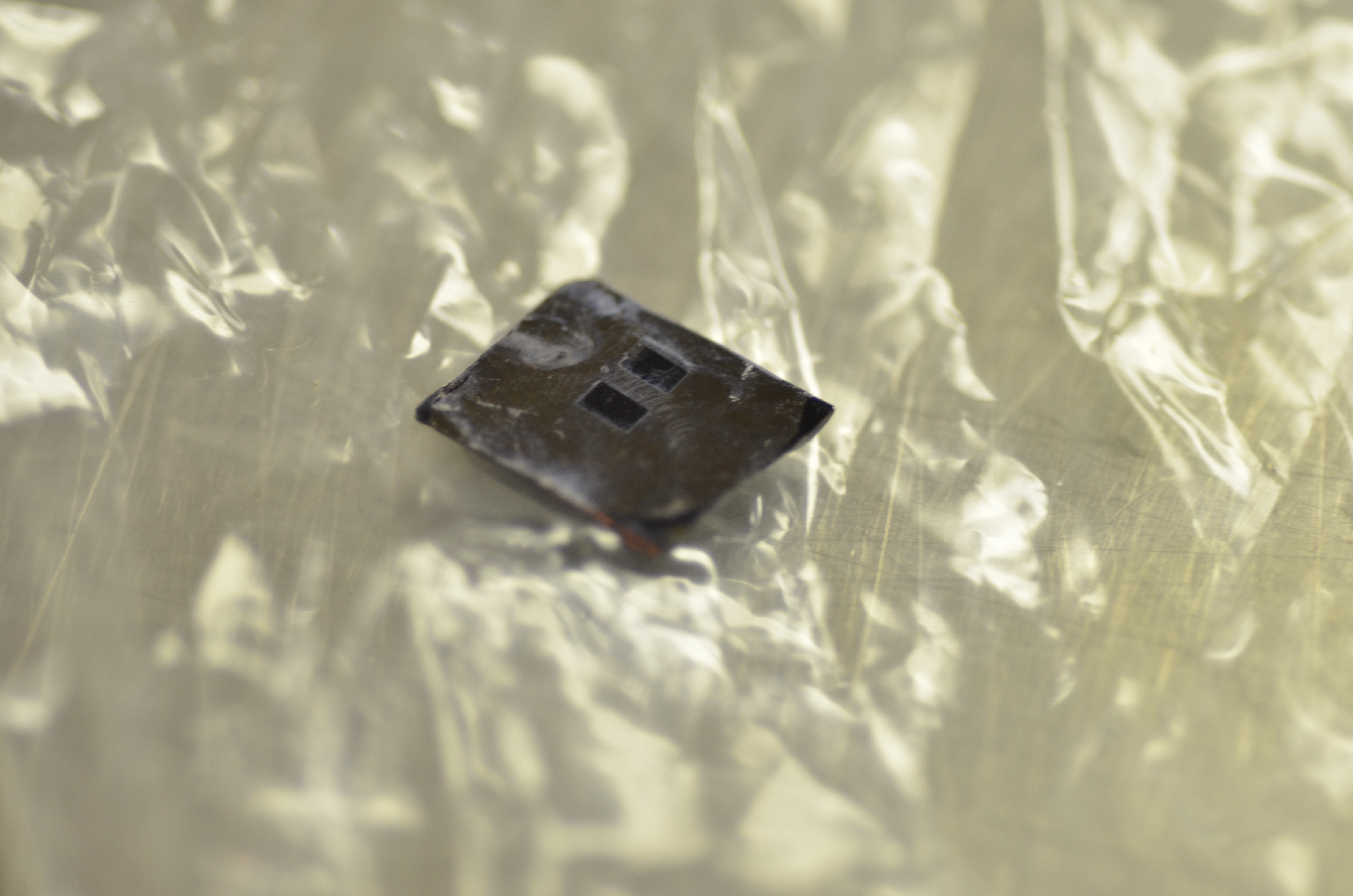
Tall particles can easily short out the thin gate oxide in these devices, as shown under my SEM. This poses an issue for making such devices in a garage; the gate oxides must be grown thicker to mitigate shorted devices which leads to a higher threshold voltage for the FET.
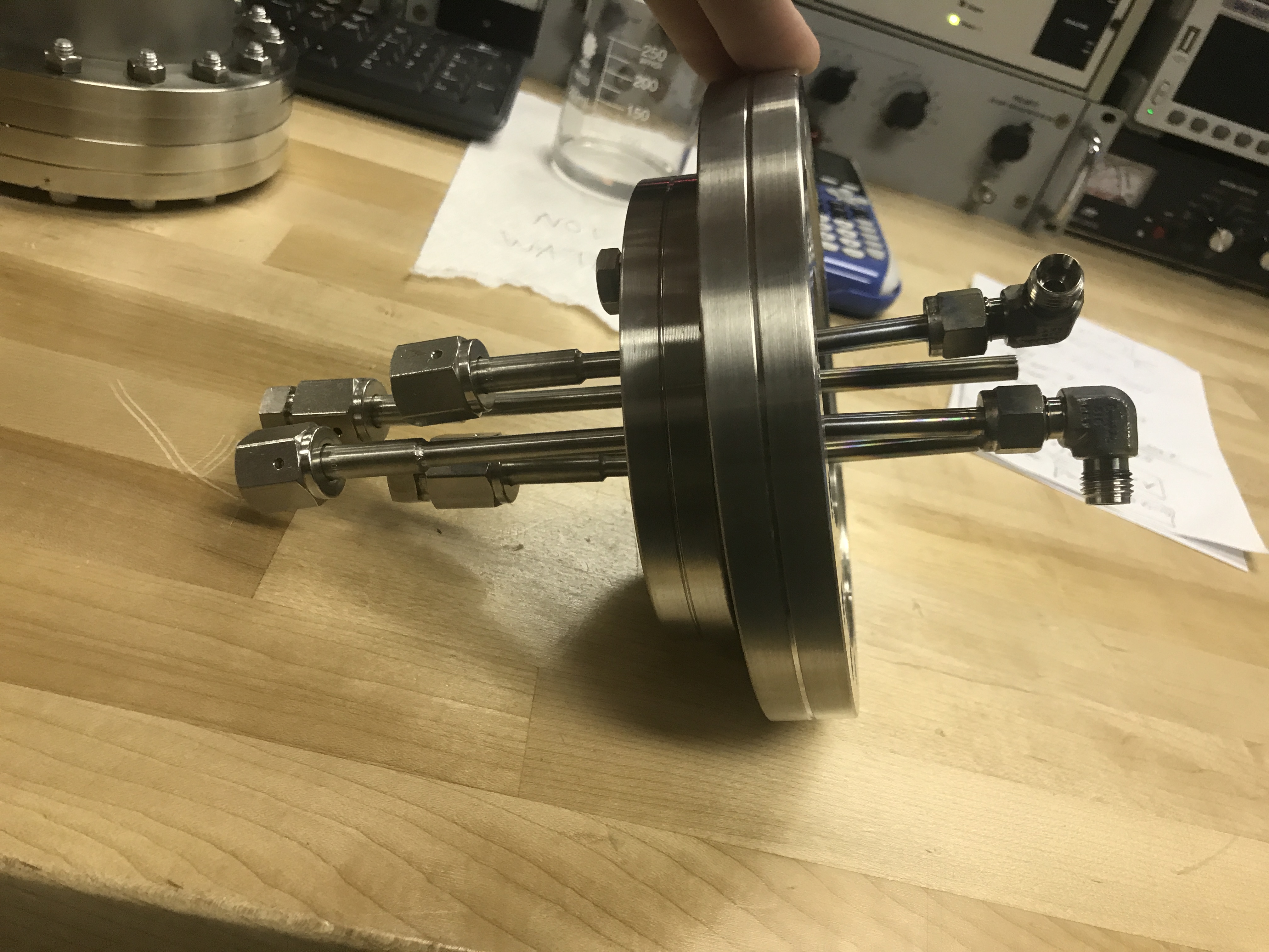
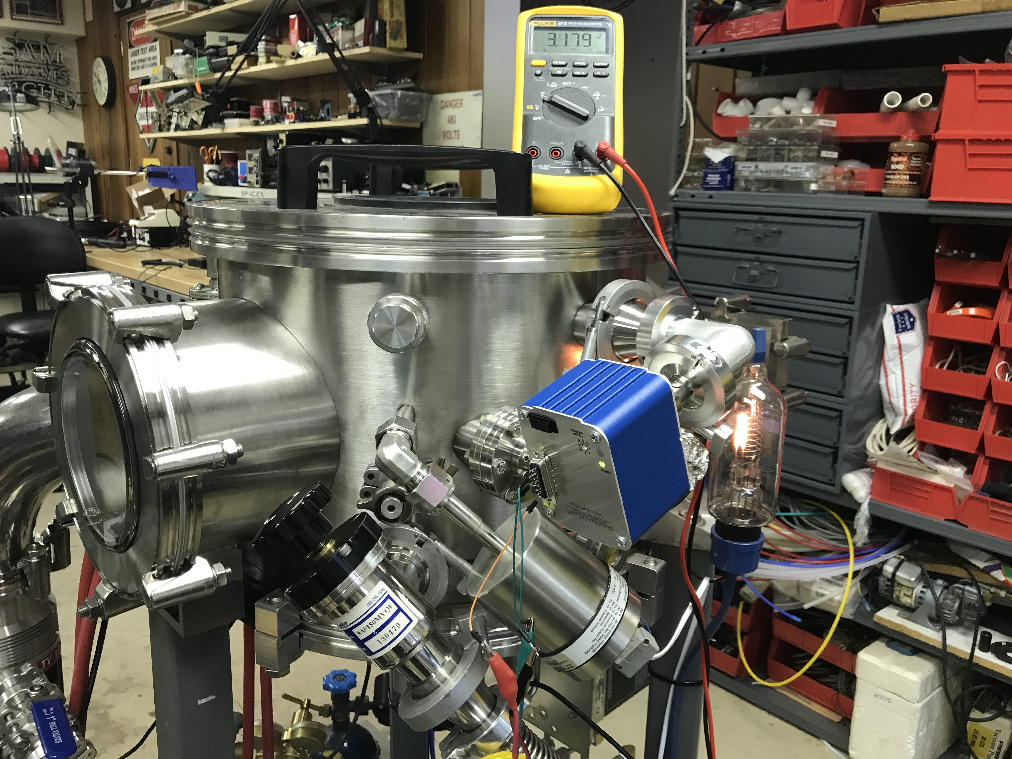
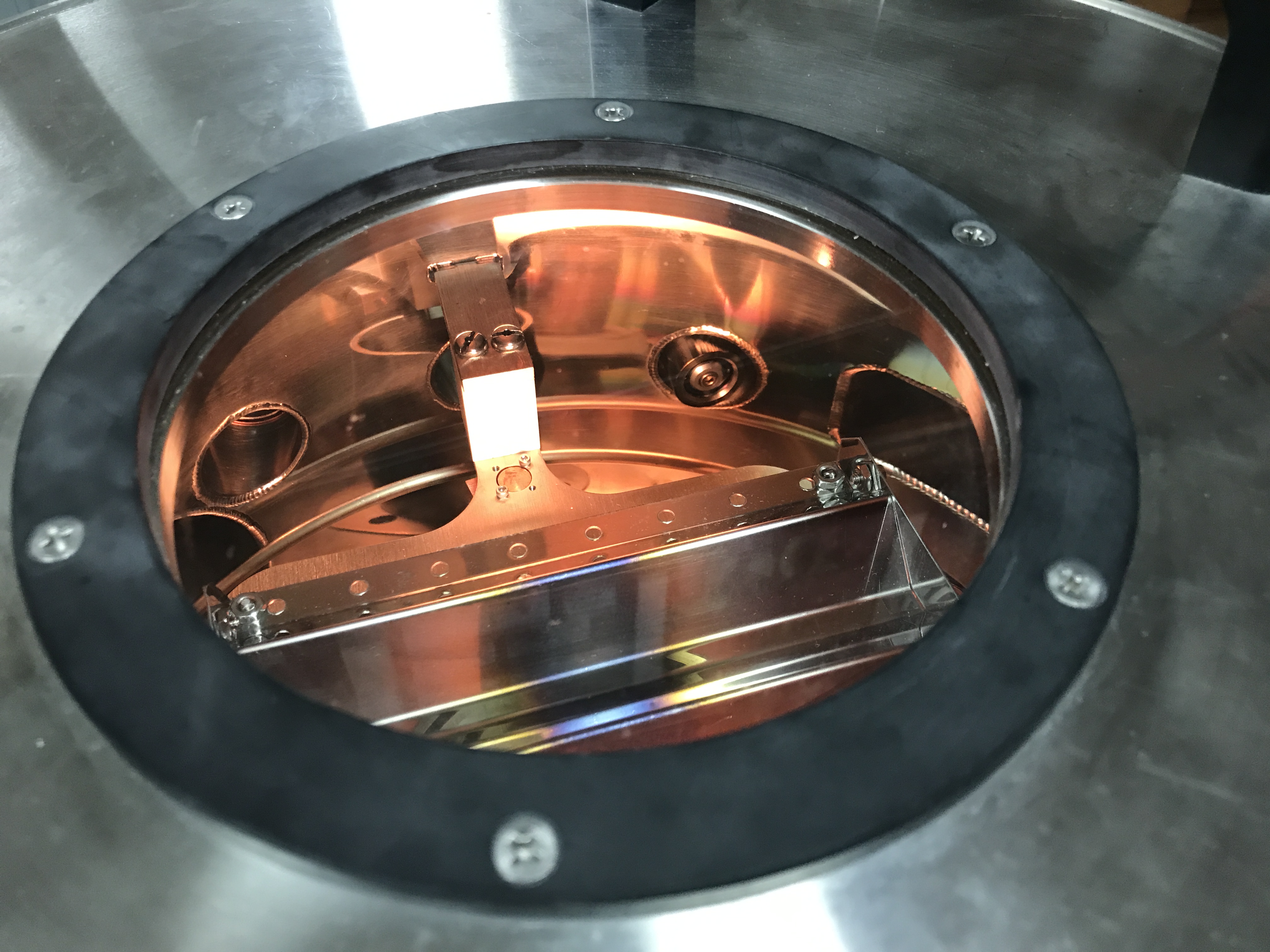
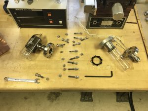
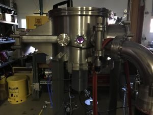
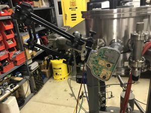
A small, modular, and versatile chamber was constructed for plasma and other research experiments. The main vacuum manifold can be configured with multiple feedthroughs in either standalone vacuum mode or connected to a large chamber. The front is a 6″ CF viewport that can be swapped for a gas feedthrough assembly.
High vacuum parts
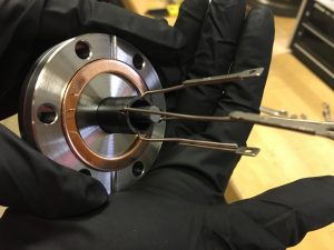
MIL-SPEC feedthrough
Viewport
Gas feedthrough
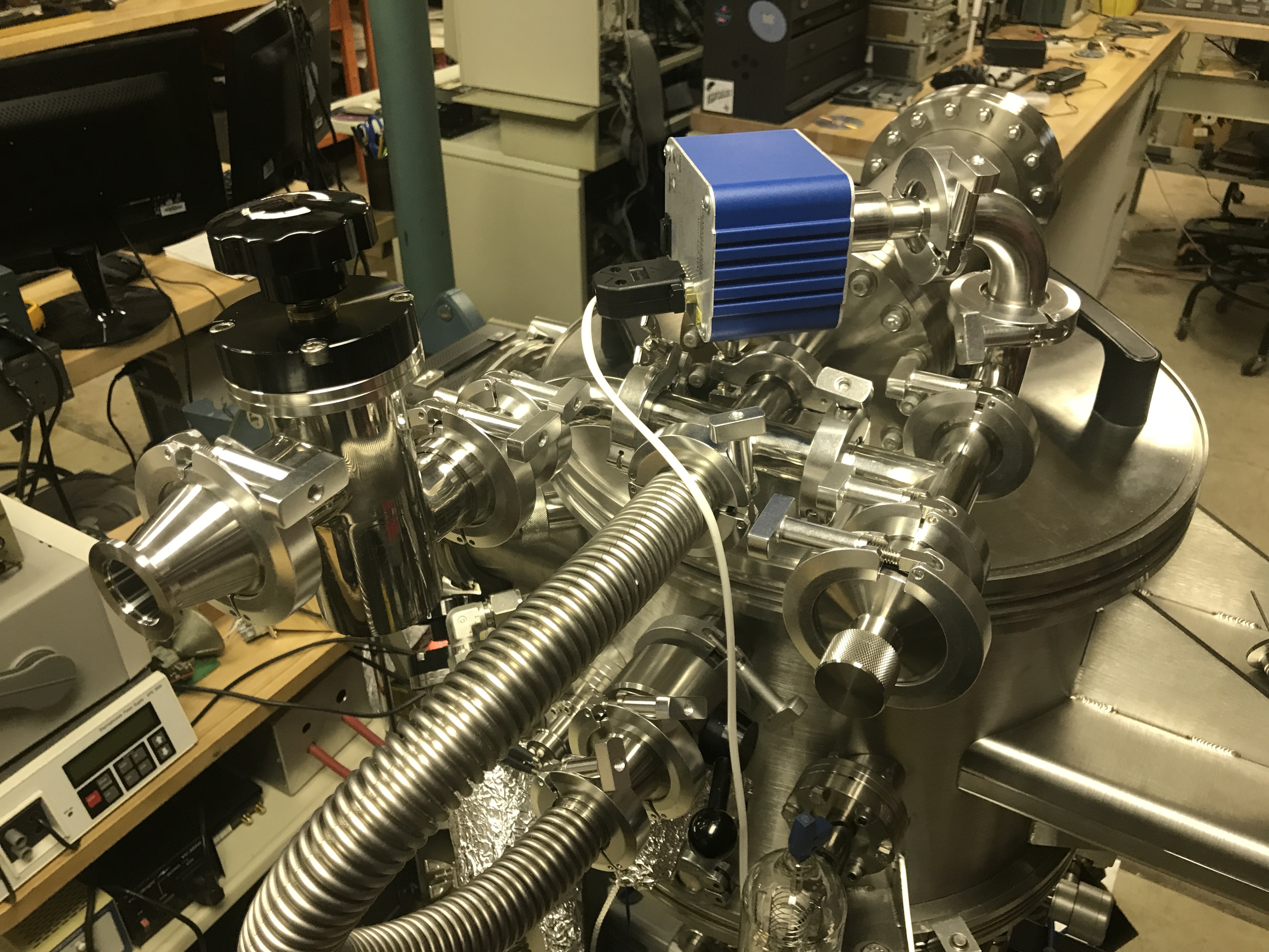
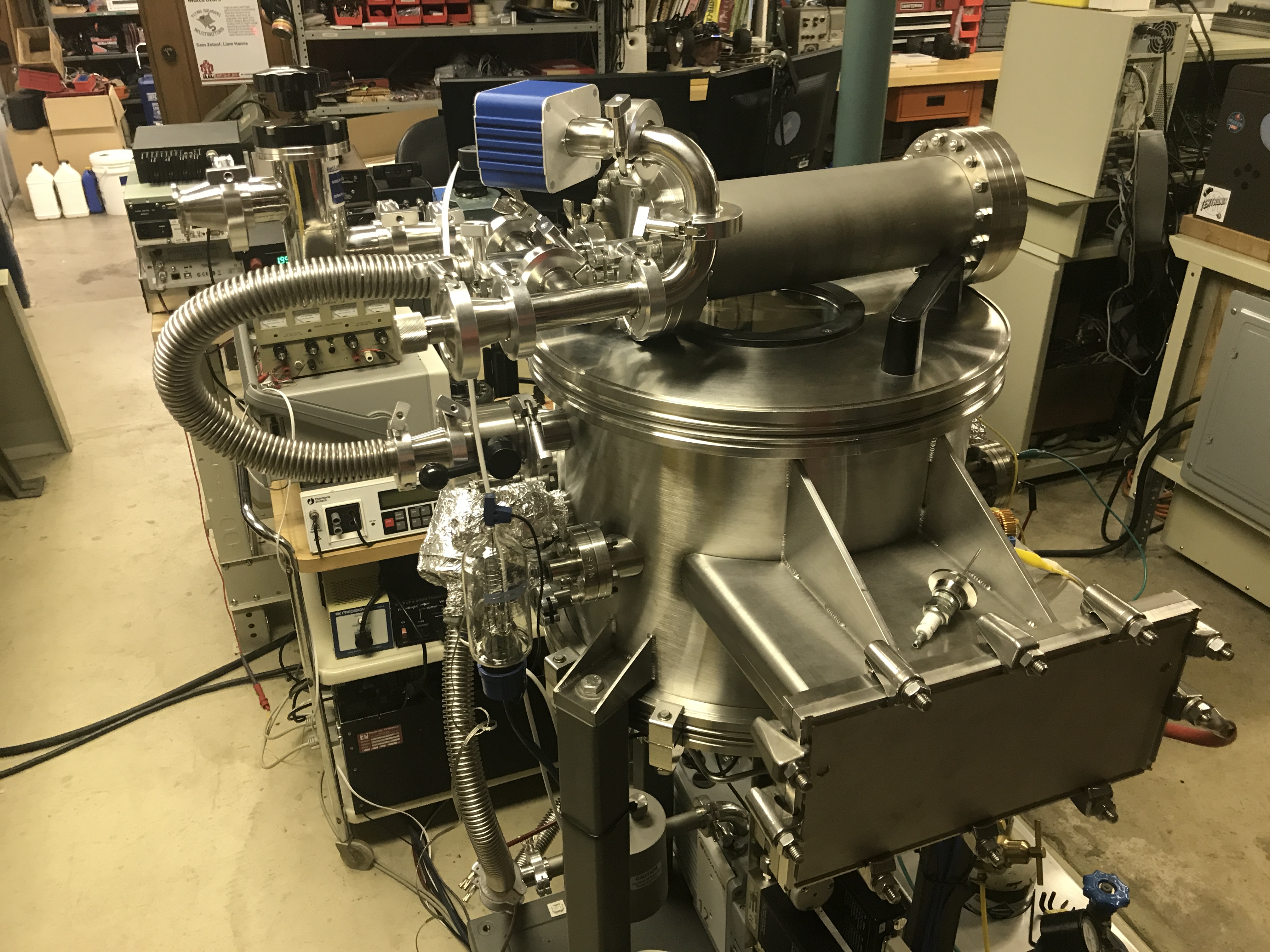
Conductance experiment
Conductance experiment
The chamber is being used right now to study simulate vacuum conductance and pressure gradients across larger chamber systems such as an ion implanter with a turbo pump on one end and an ion source and MFC gas flow far away from the pump. The gas flow creates a higher pressure in the ion source chamber and, in theory, allows for low energy beam transport and acceleration into a much lower pressure substrate/target chamber (in the case of an ion implanter).
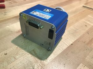
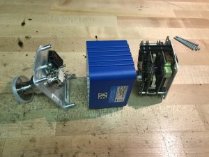
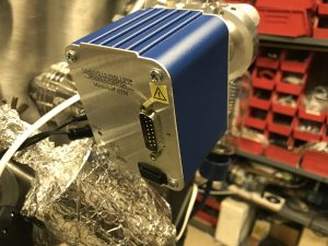
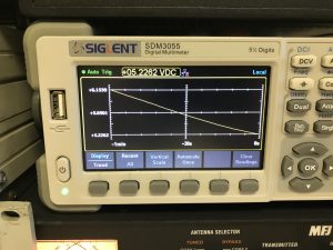
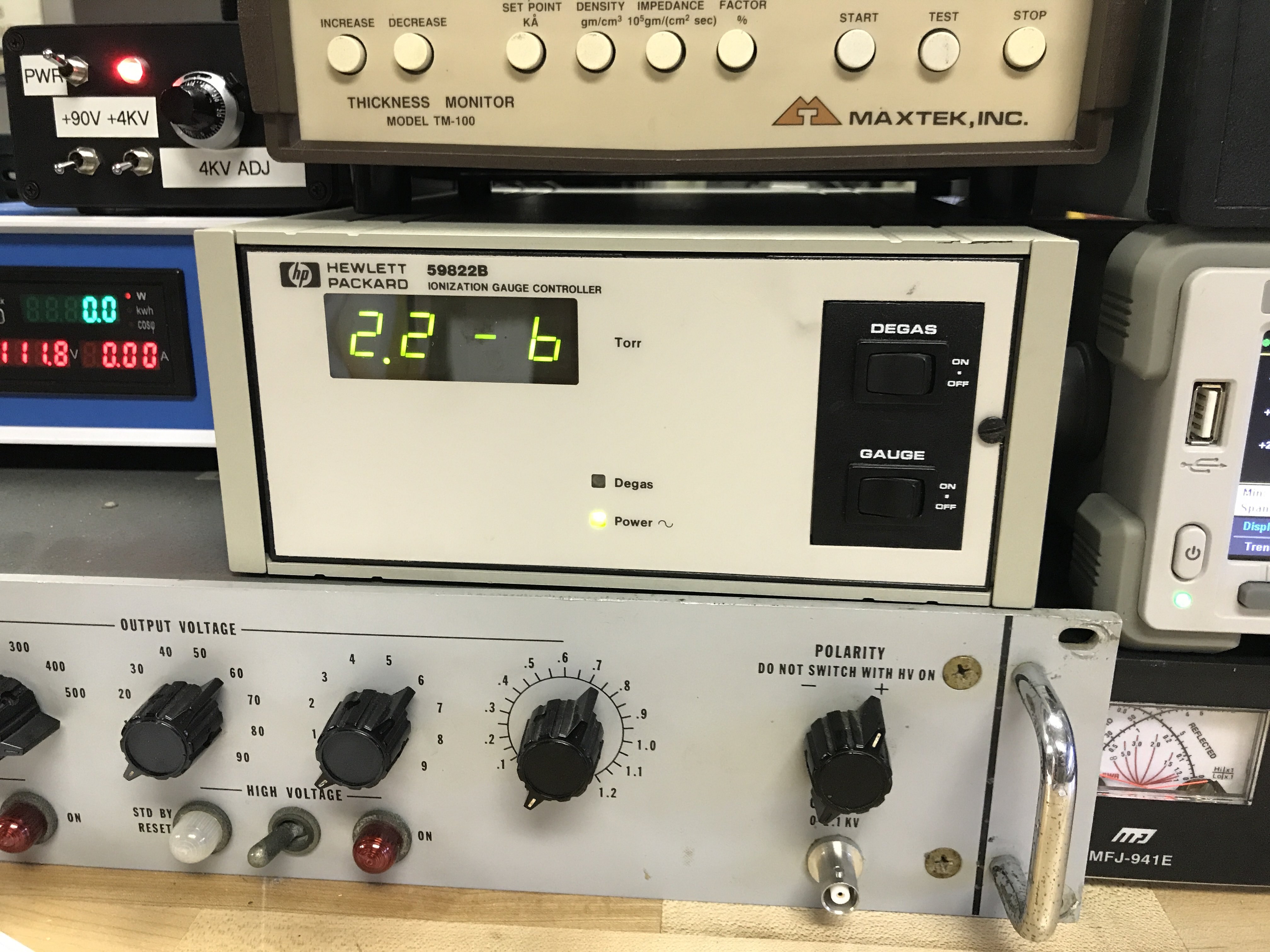
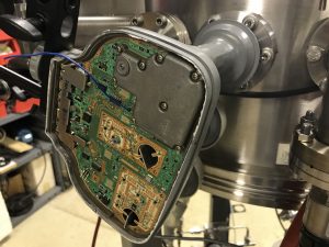
The Micro Ion Gauge ATM is an awesome gauge that is extremely sensitive and reads from atmospheric pressure down to 1e-9 torr switching seamlessly through a range of 4 different vacuum gauges. It has an analog voltage output from 7volts down to 0.5v logarithmic to the pressure. This gauge had very bad noise issues, the voltage output moved with pressure change but was not useable due to the analog output swinging ~ +/- 0.25 volts multiple times per second.
Micro Ion Gauge
Micro Ion Gauge
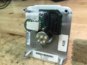
Gauge assembly
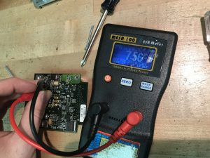
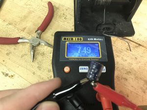
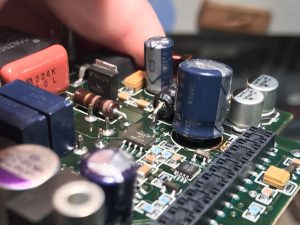
High voltage transformer
High cap ESR
High cap ESR
Electrolyte Leakage
Happy Gauge
Happy Curve
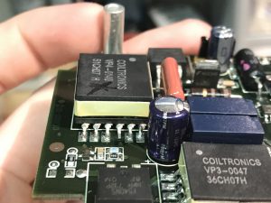
The problem was found to be bad electrolytic caps, as expected. They exhibited high ESR, Low DC resistance, puffed up vent/tops, and electrolyte leakage on the PCB.
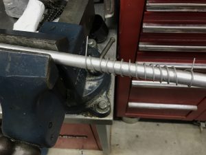
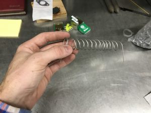
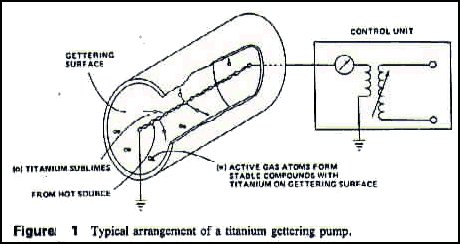
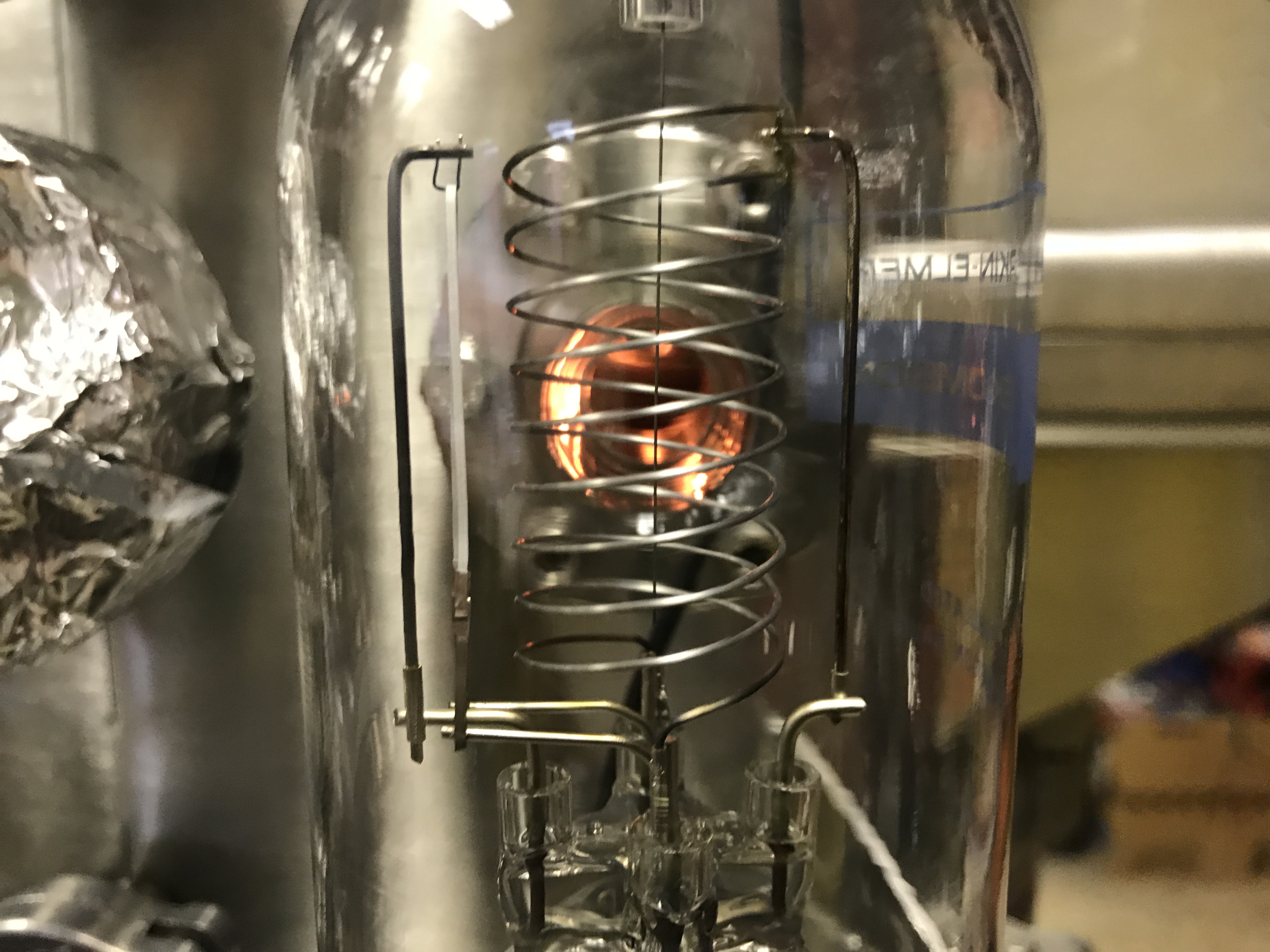
A quick attempt making a titanium sublimation pump. Ti welding rod was bent into a coil around aluminum round stock and placed across 30-50 amps in high vacuum yielding successful results. Chamber was roughed down to 20mTorr then pumped with turbo to 1e-5 and briefly baked out. More testing will be done and results will be posted along with an updated design with shielding to make it into an actual pump rather than depositing all over the chamber walls.
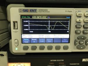
Pumping Curve
During testing I experienced a strange pumping curve a few times as shown in the last picture where the filament while heated at 50 amps seemed to out gas twice before reaching sublimation.
Ti Welding Rod
Ti Welding Rod
Ti Coil
30 amps
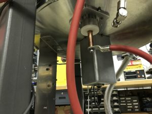
Feedthrough
Mysterious double out gas
(Click on image to enlarge)
The basic idea of a TSP or getter pump is that the filament is heated past 900 degrees c with a high current across it. The filament first out gases and raises the chamber pressure, but then reaches sublimation pressure where it begins to form a thin volatile coating of Ti on the chamber walls.
Titanium, in this heated state, will readily combine with gaseous specious in the chamber to form a more stable coating and the gas molecules in the chamber basically get incorporated into a thin film on the chamber walls and trapped. The filament current is cycled for highest effectiveness. A rewound MOT is used for high current supply.
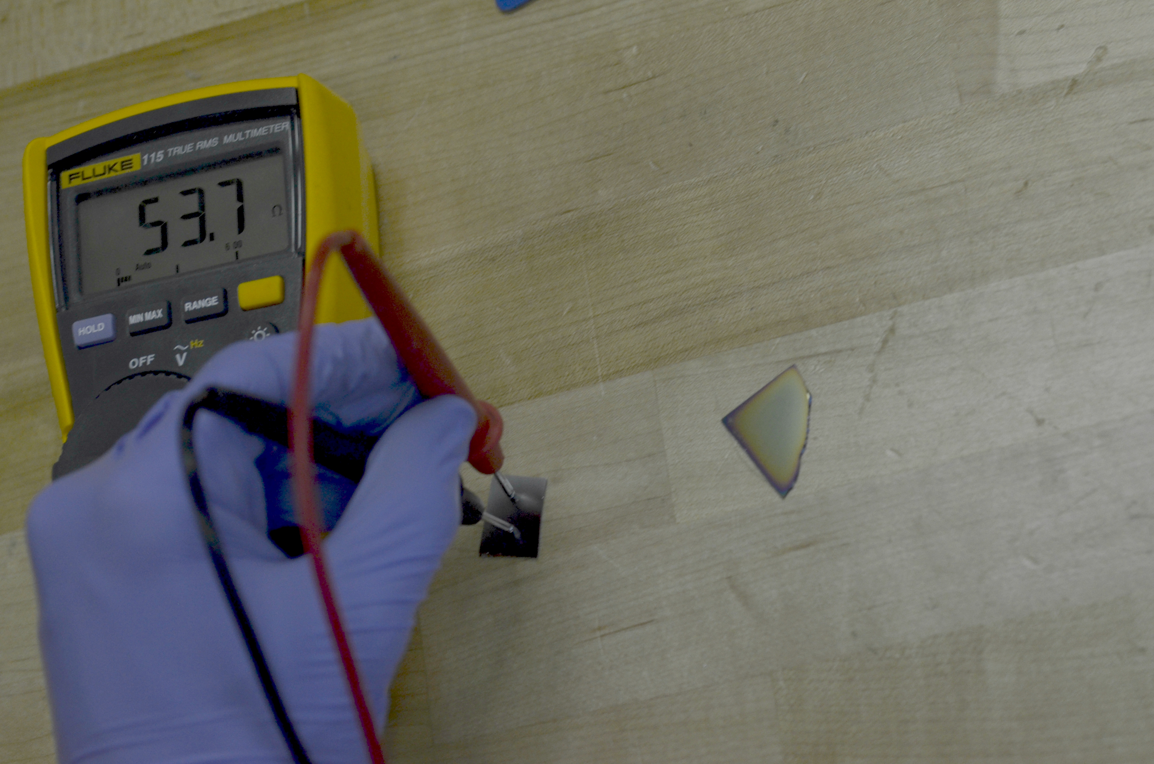
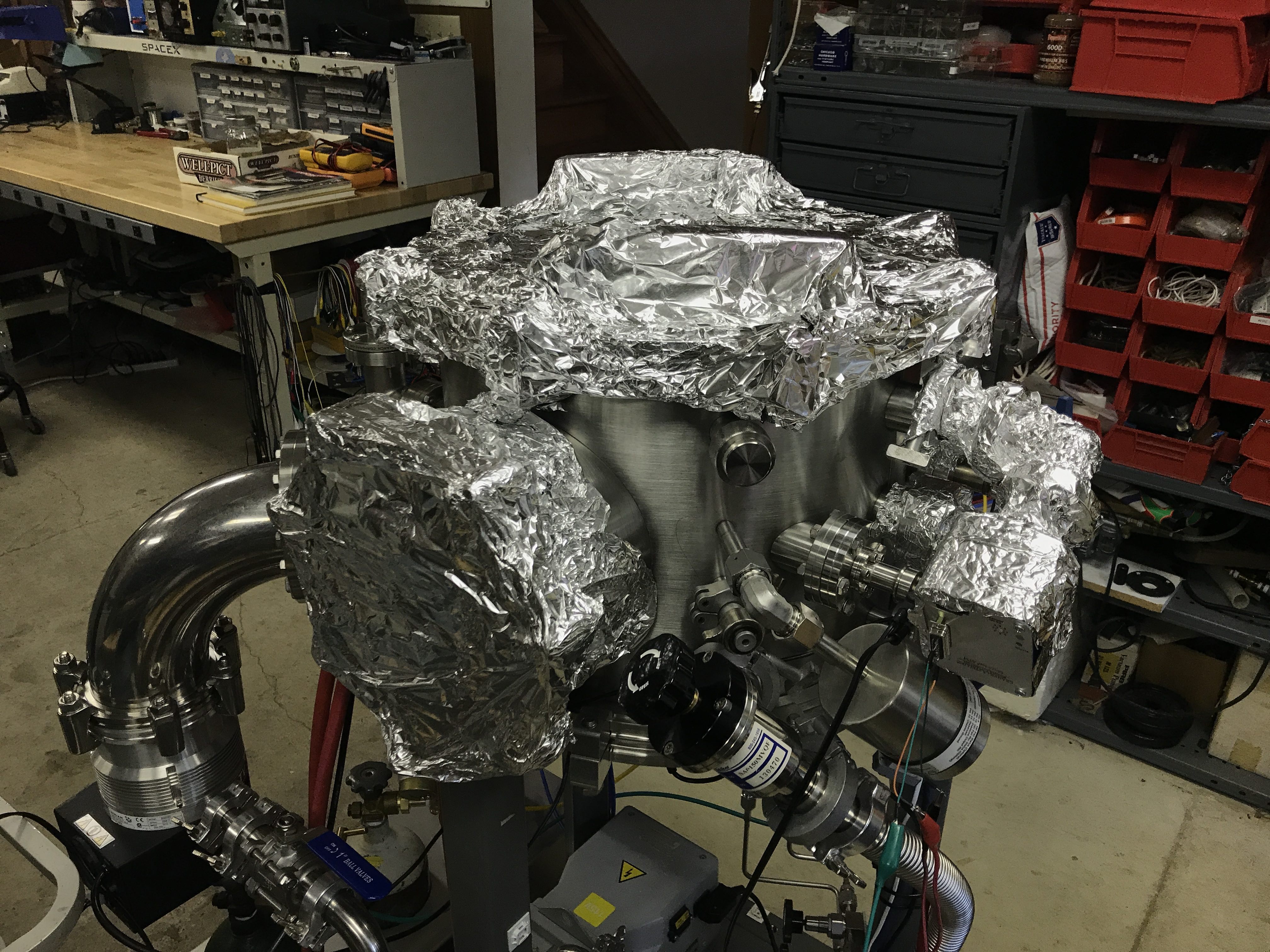
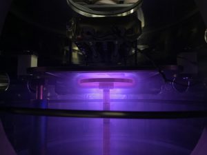
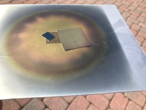
Progress in developing the metalization process for the home chip lab. DC and RF sputtering is used and the process will be refined more and then I will move on to the wet process with etching metal through resist mask, etc.
Sample is scratched with a razor and surface roughness is measured with a KLA Tencor Stylus Profiler. Surface is extremely rough and best interpretation of the data leads me to believe the thickness of the sputtered film is approximately 0.492um.
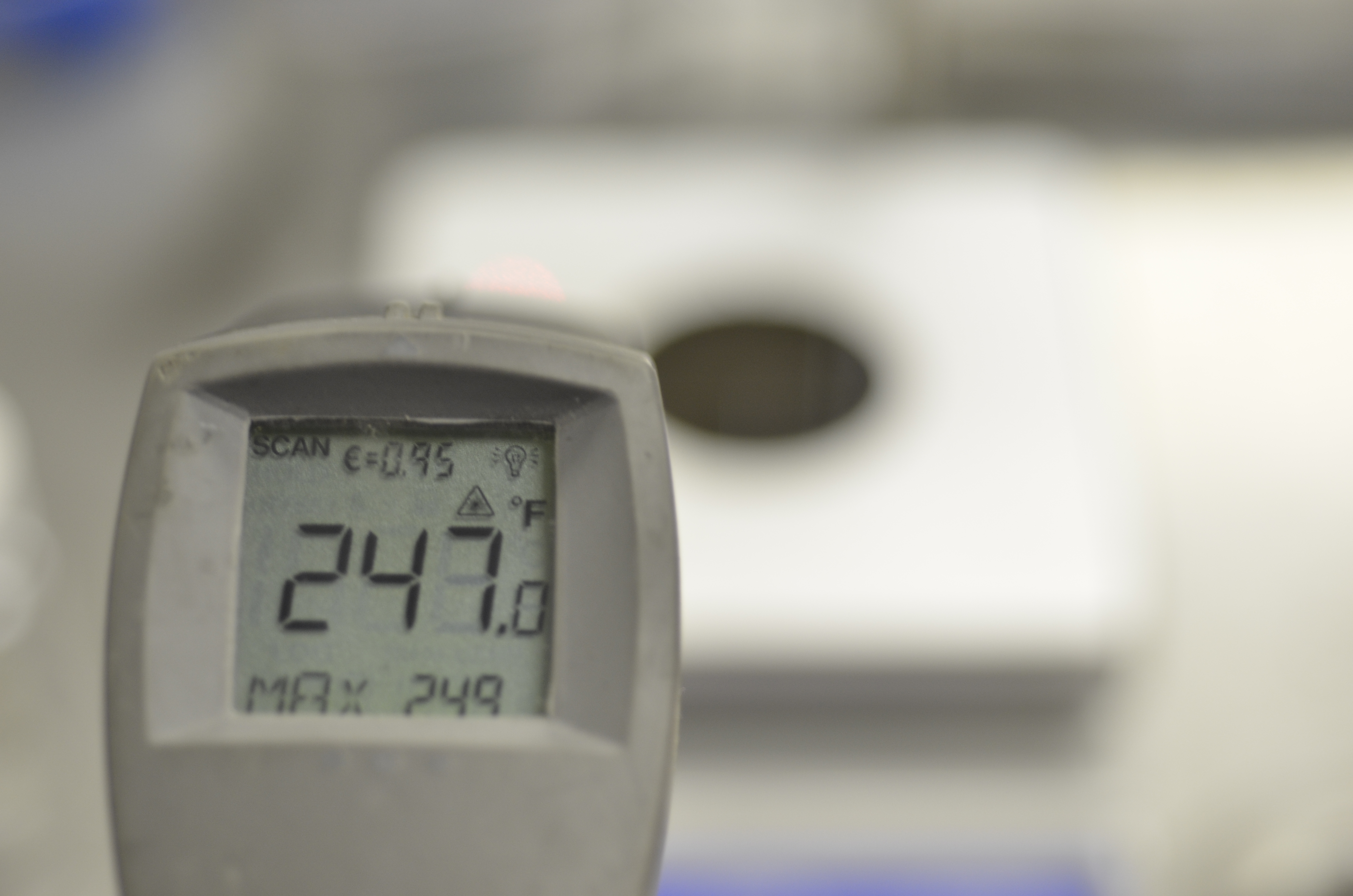
Two internal radiant infrared heat lamps and external resistive heating elements are used to bakeout the vacuum system for 24 hours allowing for ion pump operation. Normally when the chamber is full of unwanted moisture and impurities ionizing gas in the chamber will lead to a sharp increase in pressure due to plasma cleaning of the chamber walls and subsequent release of gas molecules.
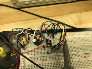
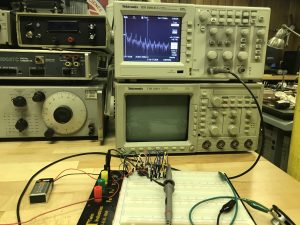
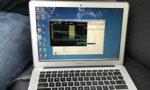
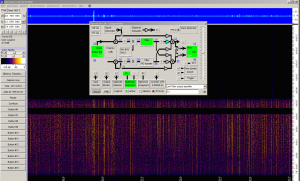
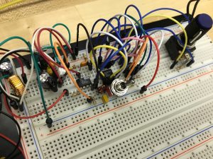
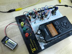
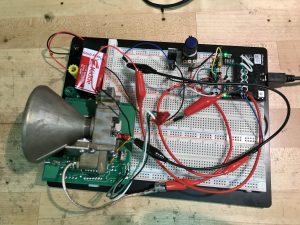
Quick prototype of a VLF/ELF receiver with two stage low noise amplifier and passive RC bandpass filtering. First stage has a gain of 180 then is fed to a lowpass and highpass filter then to another opamp with adjustable gain up to 500. Resulting signal is sent to a Focusrite Scarlet i2i 24bit USB audio interface and sampled at 192KHz.
This simple preamplifier can easily pick out the “fire crackling” of lightning strikes around the world form the noise floor and can easily resolve other natural low frequency radio phenomena such as “”whistlers”. Active bandpass filtering and 60Hz notch filter will be added as well as a shielding enclosure and low noise Analog Devices OP270 or similar opamps will be used in another iteration of the design.
Antenna used was two large screw drivers inserted into the ground soil separated by about 50 feet in the woods 1/4 mile from any house or power lines. 60Hz noise was exceptionally low considering only passive RC filtering was used which has high and low -3dB points far away from what you actually design the cutoff frequencies of the filter to be.
This frontend contained no input protection in the form of glow discharge neon lamp, clamping diodes, thermistor, MOV, fuse, etc. Next design will incorporate multiple such devices however it is not a great priority for testing because I am using the screwdriver ground probes for antenna which is less susceptible to high voltage buildup in storms as a whip or dipole antenna.
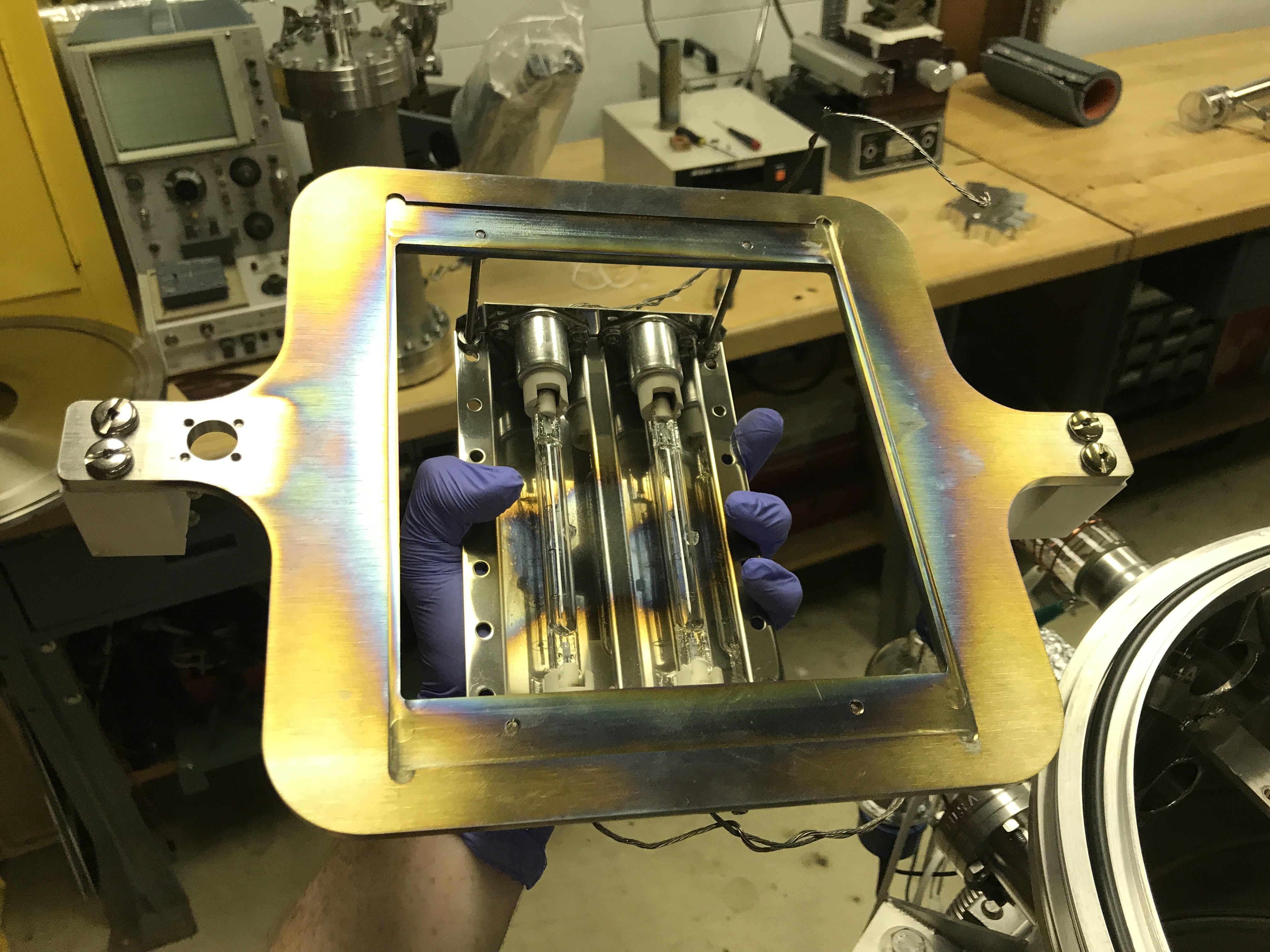
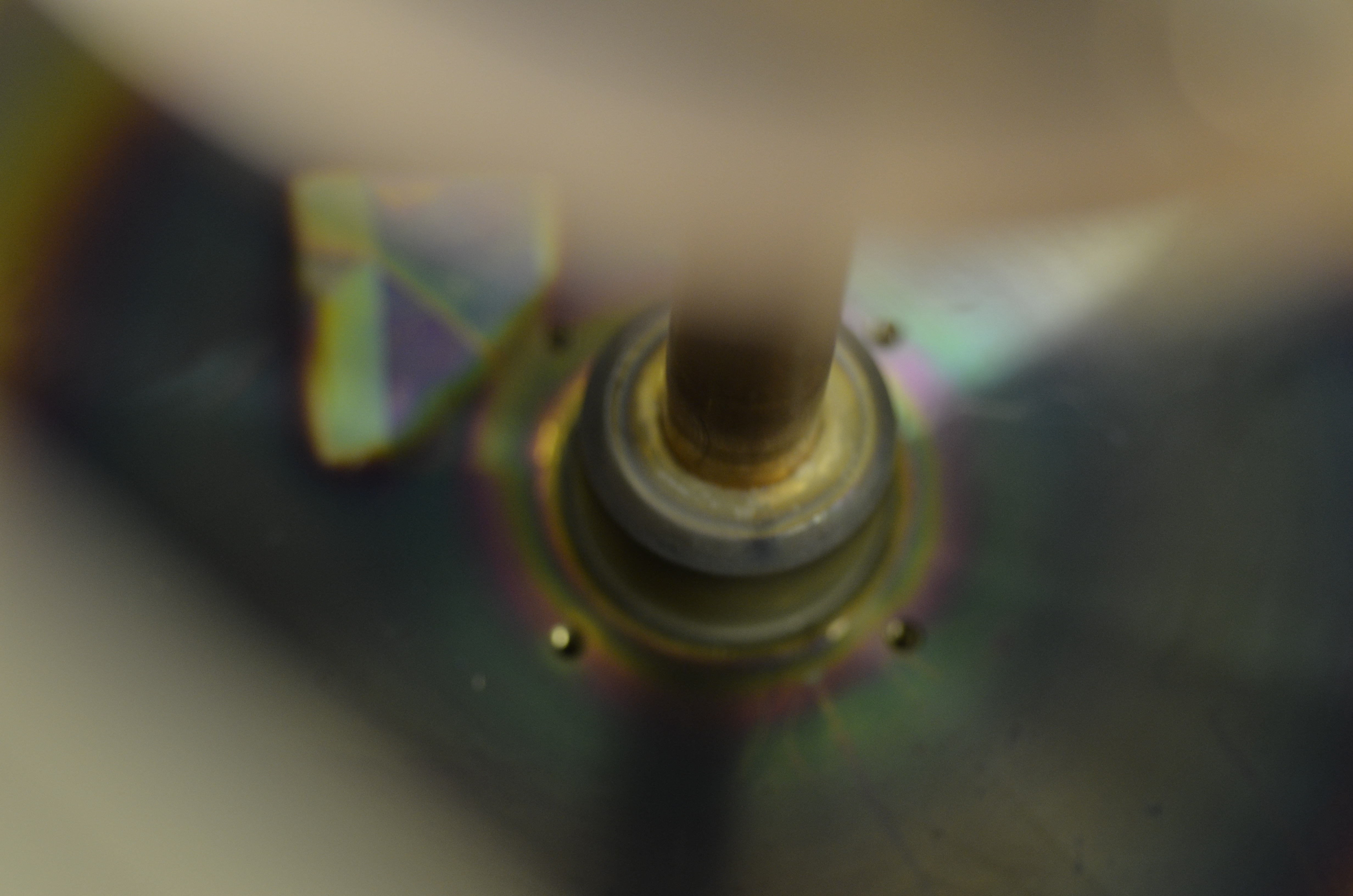
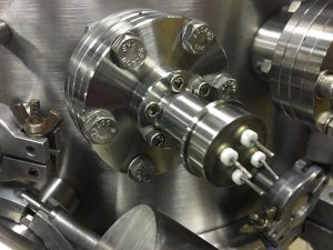
I machined a delrin insulator with fiberglass center rod for the CF 4 pin electrical feedthrough to provide power to the two incandescent substrate heaters in my new sputtering setup and to allow for instrumentation hookup.
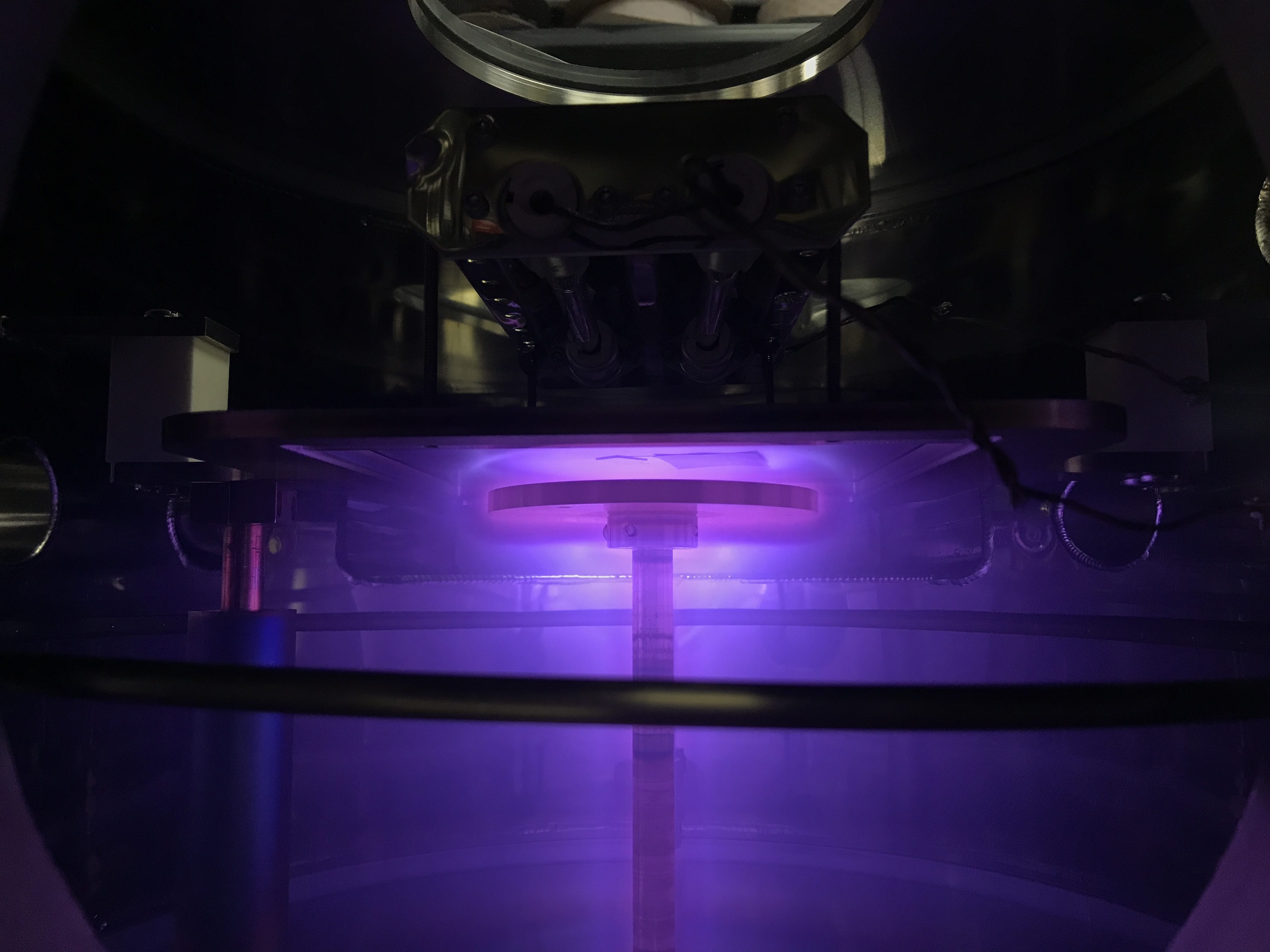
New sputtering setup has dual substrate heaters as well as insulated feedthroughs for both target and substrate so that it can operate in DC, RF, Bias sputtering modes, or any combination therein. A quartz microbalance thickness monitor will be added soon.
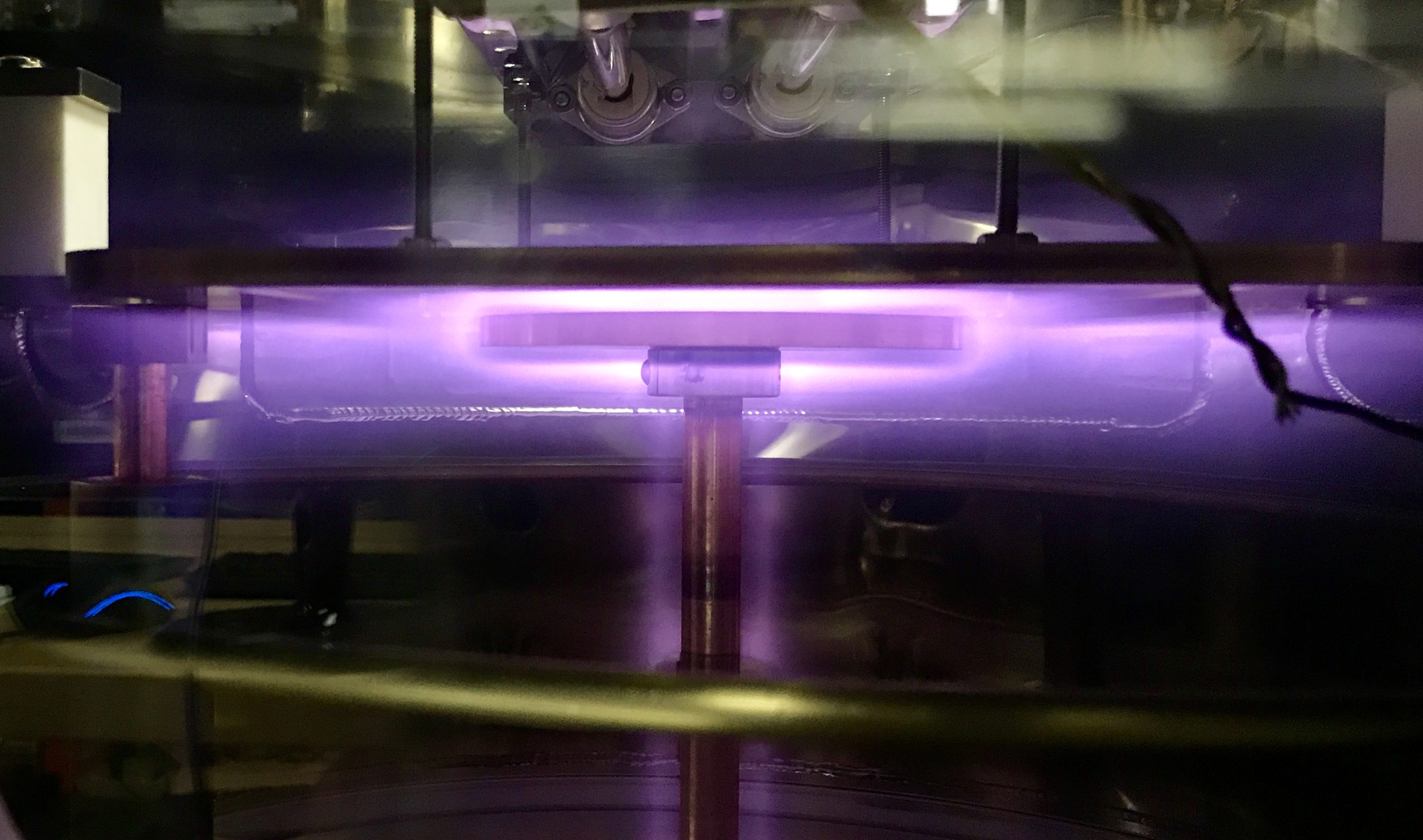
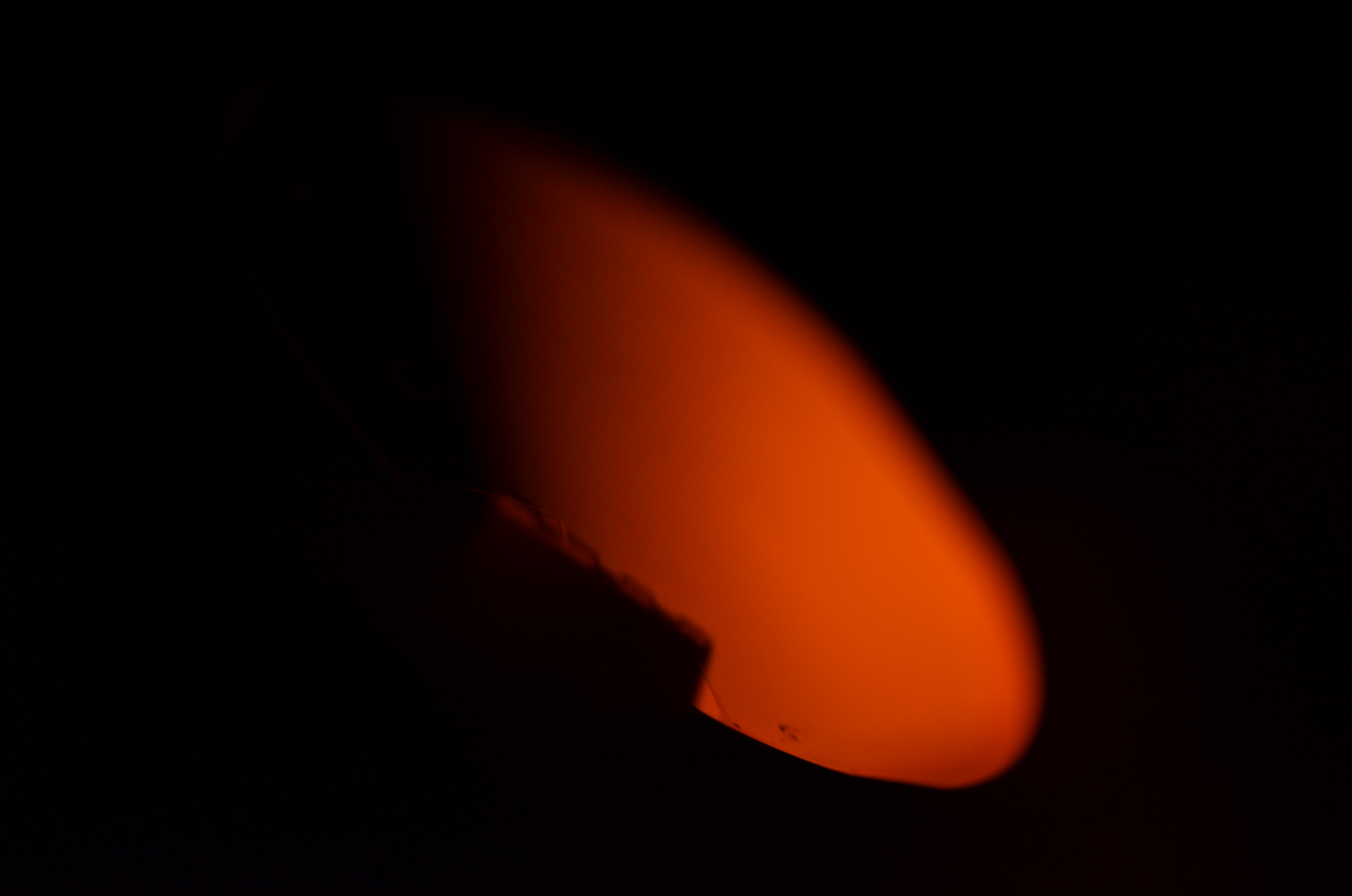
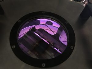
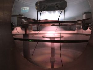
The second to last image shows multiple colors in glow discharge during sputtering possibly due to DC bias. Bottom and top electrodes are both at different potentials with respect to chamber ground, so it is possible that different gasses are ionized due to differences in ionization energies of the residual gaseous species.
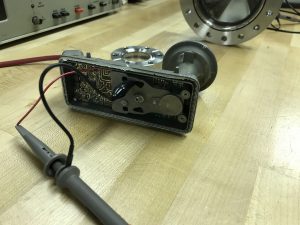
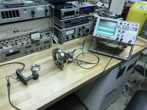
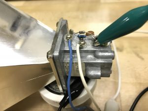
Prototyping of a microwave interferometer setup has begun using modified police radar and satellite television parts, namely Gunn Diode oscillators (gunnplexer) and LNBs with dielectric resonant oscillators as well as PLL synthesized ones. Tests are being conducted at X, Ku, and K bands. The goal of this is to non-intrusively measure electron density in plasmas in my chamber. Results of these experiments will be posted.