I modified my JEOL scanning electron microscope to not only image tiny things, but make tiny things too.

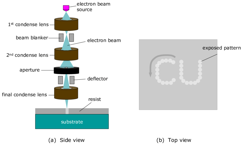
This technique is called Electron Beam Lithography. Normally, a SEM works by scanning a beam of electrons over the sample and detecting secondary electrons. In this case, I built a PC scan controller that “drives” the electron beam around and draws the image onto the sample which is coated with electron-sensitive resist.
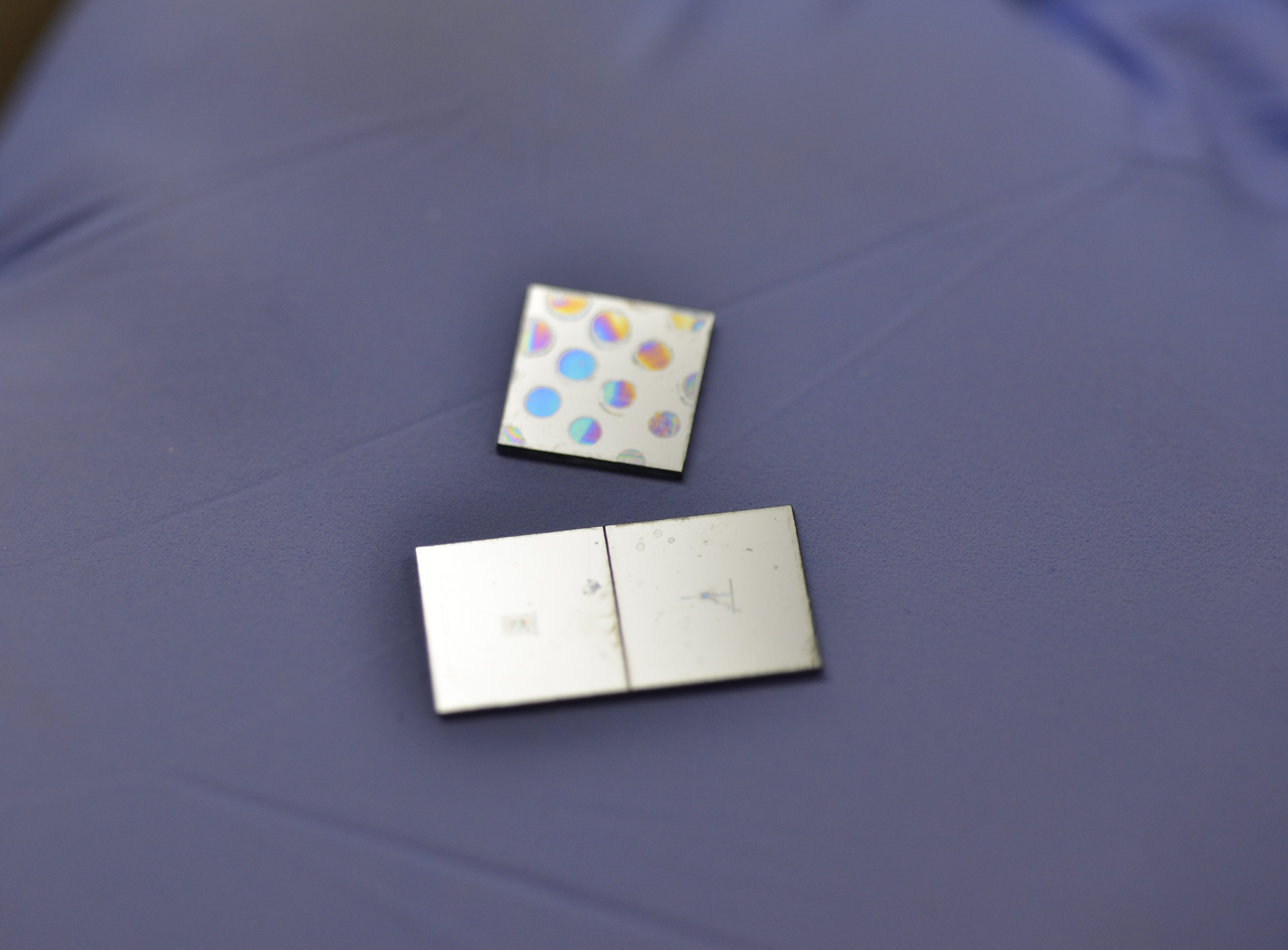
 For resist, I used SU-8 although PMMA (Acrylic) dissolved in solvent will work as well.
The scan controller uses dual 12 bit DACs. They had current outputs so a transimpedance amplifier creates +/-10v proportional to that current to drive the microscope’s external XY inputs. The controller also contains an Arduino and Altera CPLD. To turn the beam off when needed, a high voltage is generated (+2kv) and applied to a “beam blanker” inside the microscope.
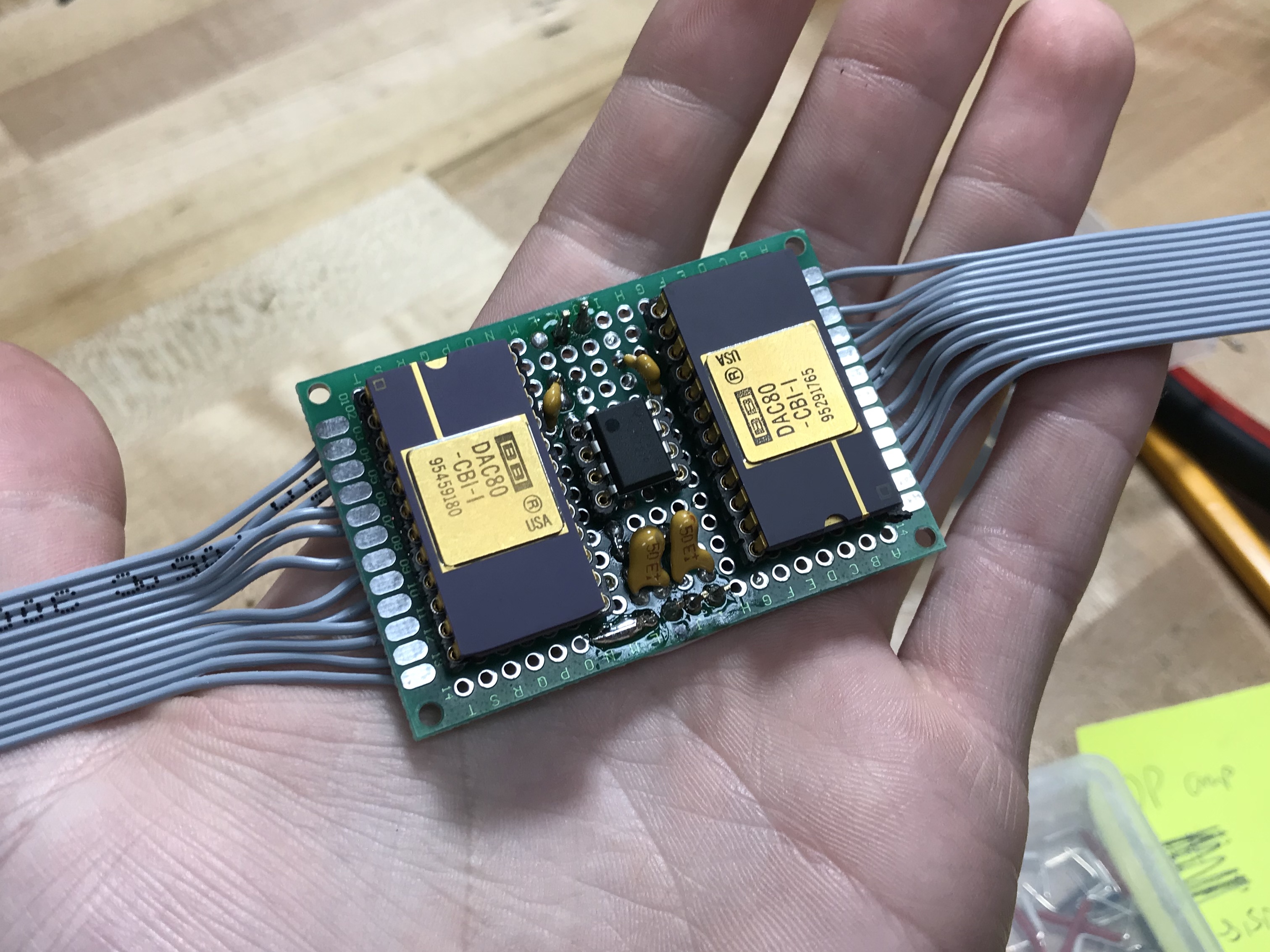


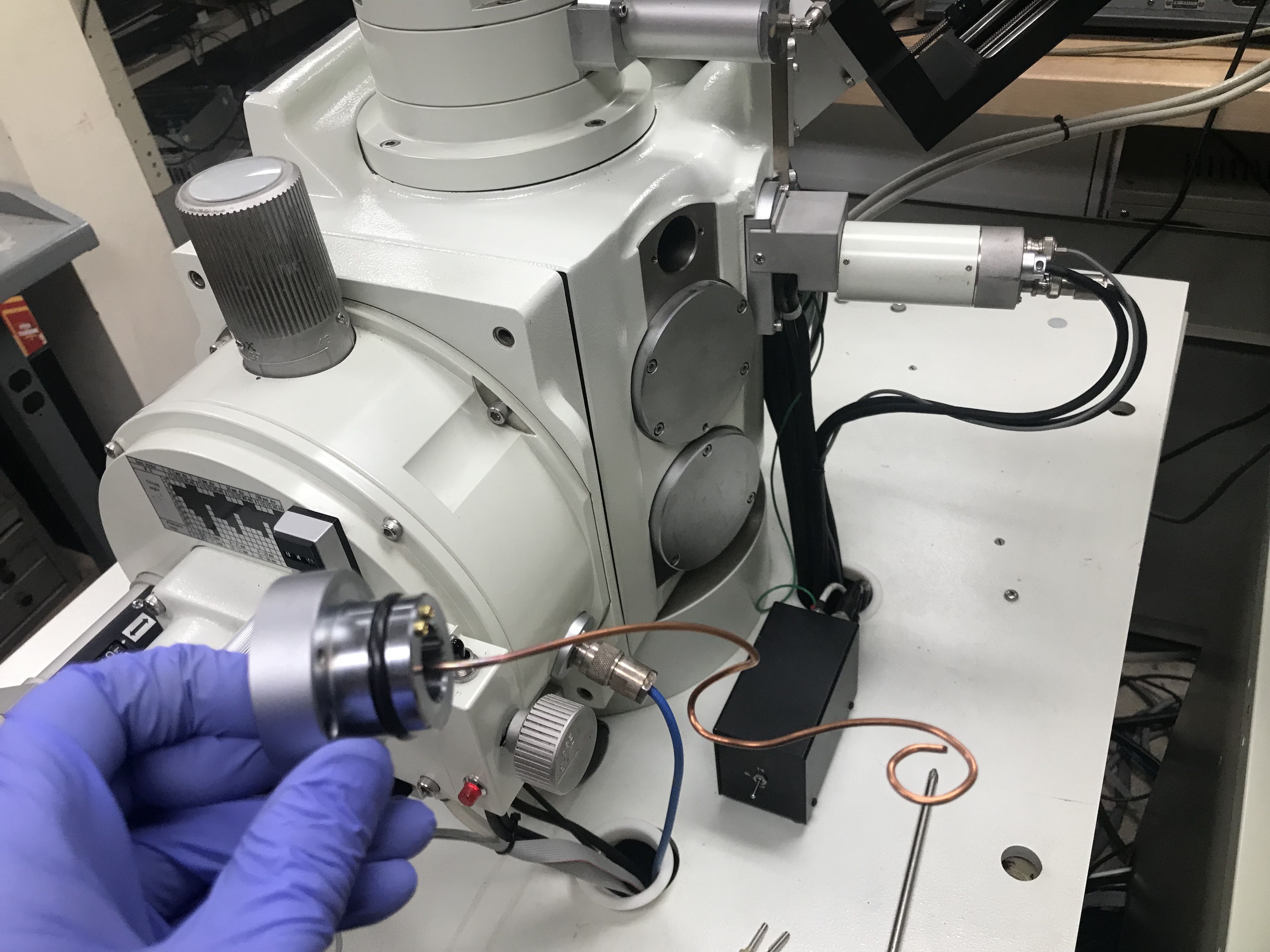


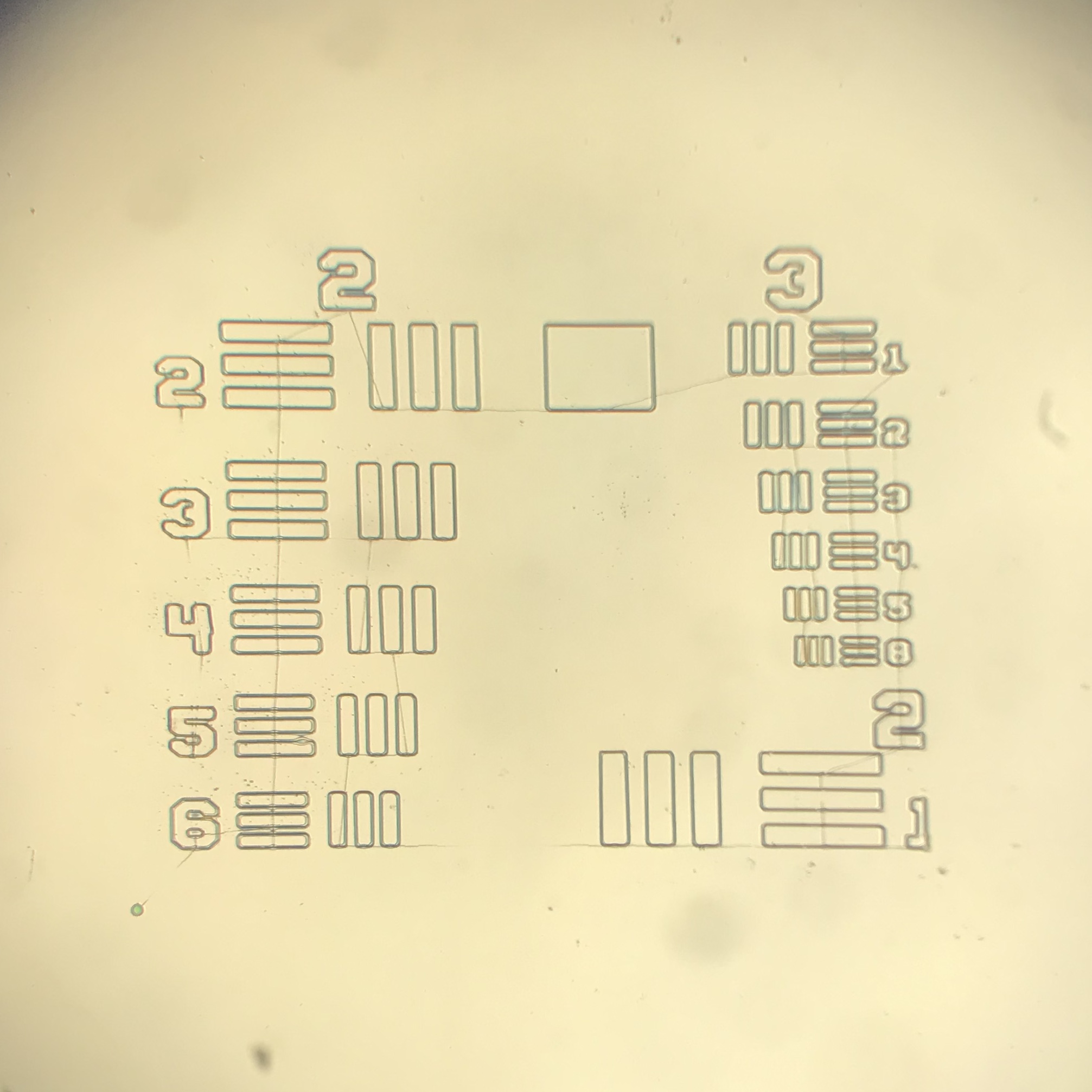


I learned that the 12 bit DACs do not nearly have enough resolution, so I will be looking at upgrading to at least 18 bits hopefully. Also, the geometry of the beam blanker is not correct to create a high electric field in its center, so the beam is only partially de-focused and never fully “turns off”.
Update (2020): New photos with improved beam blanker –


Please enable https. When i now visit your website, every single hop is able to run a zero day exploit in my browser. Please
Has there been any further progress on this? I’m quite intrigued by the possibilities of E-beam lithography for “maker-scale” chip fabrication, since its primary downside of being way too slow for mass fabrication would no longer apply if you only needed to make a few units of any particular chip design. It seems like it could allow exposure of feature sizes competitive with (relatively) recent processes, while needing much less involved tooling.