


As of now, I am doing all of my doping with spin on diffusants. Some of which are solutions of Phosphoric/boric acid in alcohol/water that I prepared myself. I find it hard to control the dopant concentration and therefore bandgap of devices so my solar cells often have a bandgap too high or too low. I thought using an actual spin on dopant would help, so I bought some P509 phosphorus glass from Filmtronics and it works about the same as the solutions I made, except it spins on much nicer.
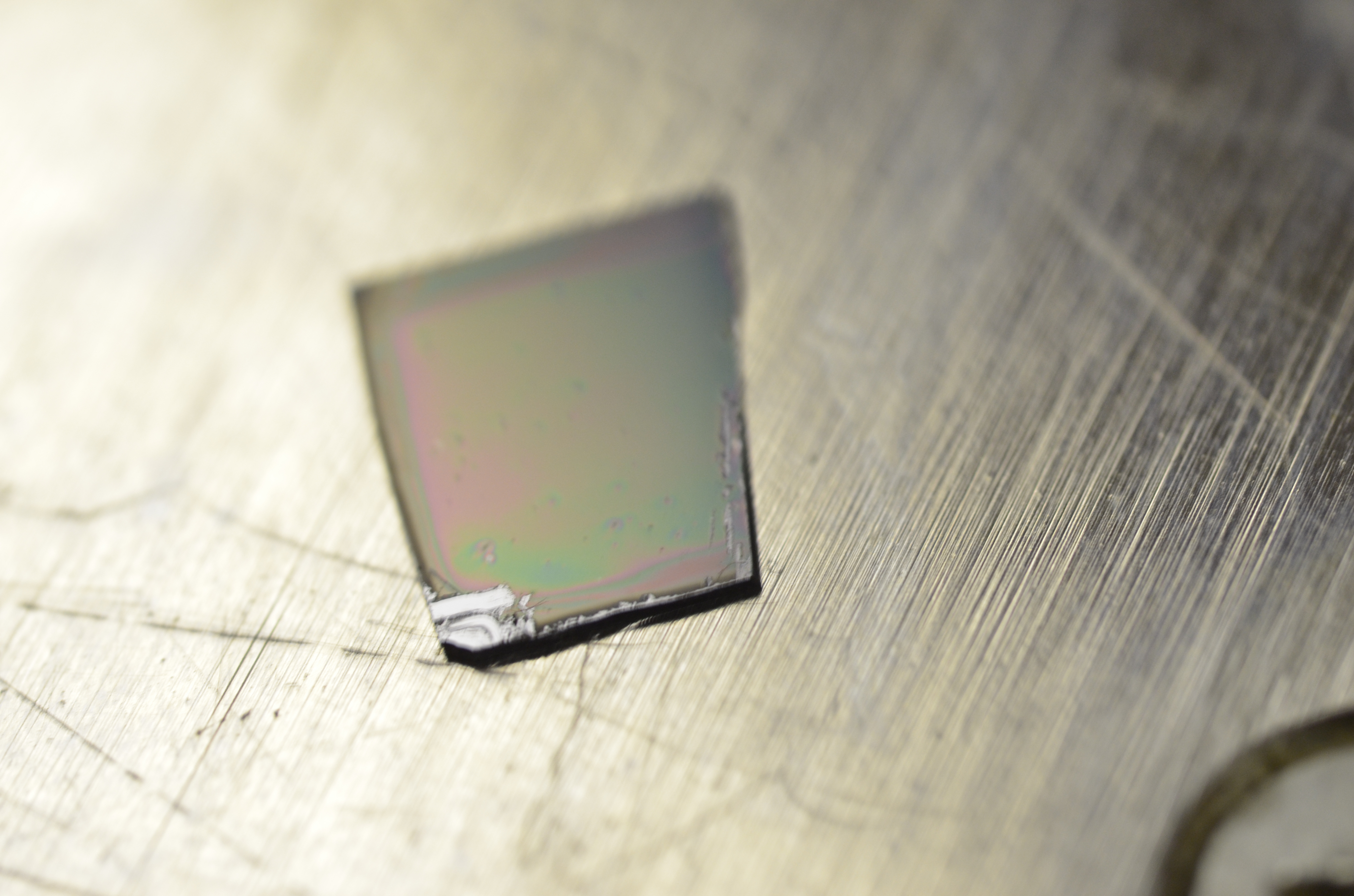
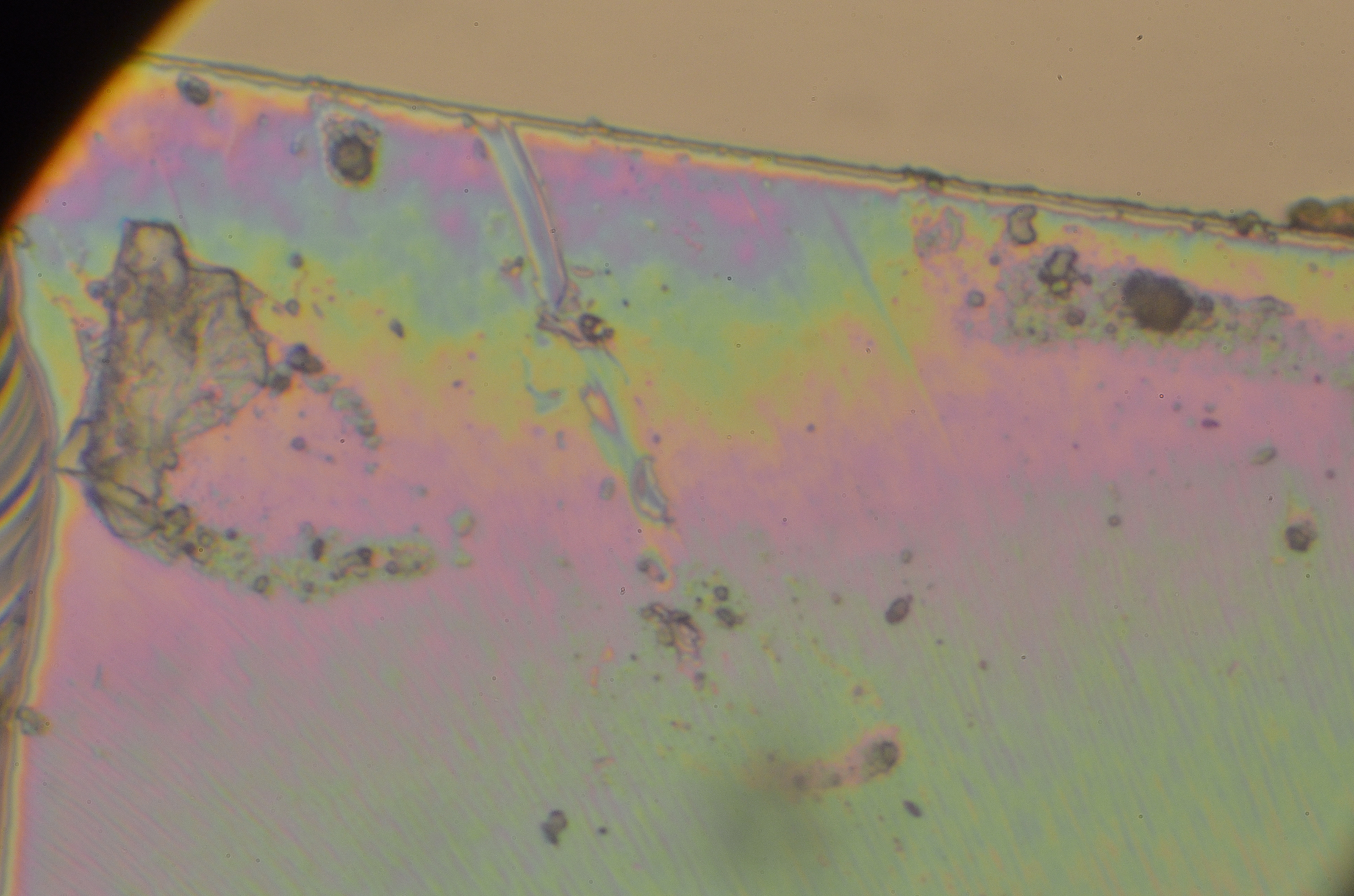
The colors you are seeing are contamination and nonuniformity in the thin film interference patterns caused by this thin glass layer after pre deposition of the spin on diffusants.


what is ‘spin on diffusant’?