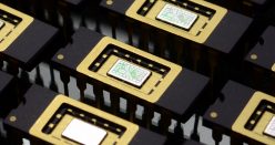
In IC fabrication it is necessary to deposit/grow and etch insulating layers of Silicon Dioxide. This presents a few problems for standard photolithographic patterning because SiO2 is hydrophilic which can cause photoresist adhesion issues and also the HF etchant attacks most photoresists. These issues combine to leave you with poor pattern definition and often complete photoresist lifting during etch.


The steps I have found to mitigate these issues are (in order): dehydration bake, HMDS vapor prime, thick resist coating, hard bake, and buffered oxide etch.
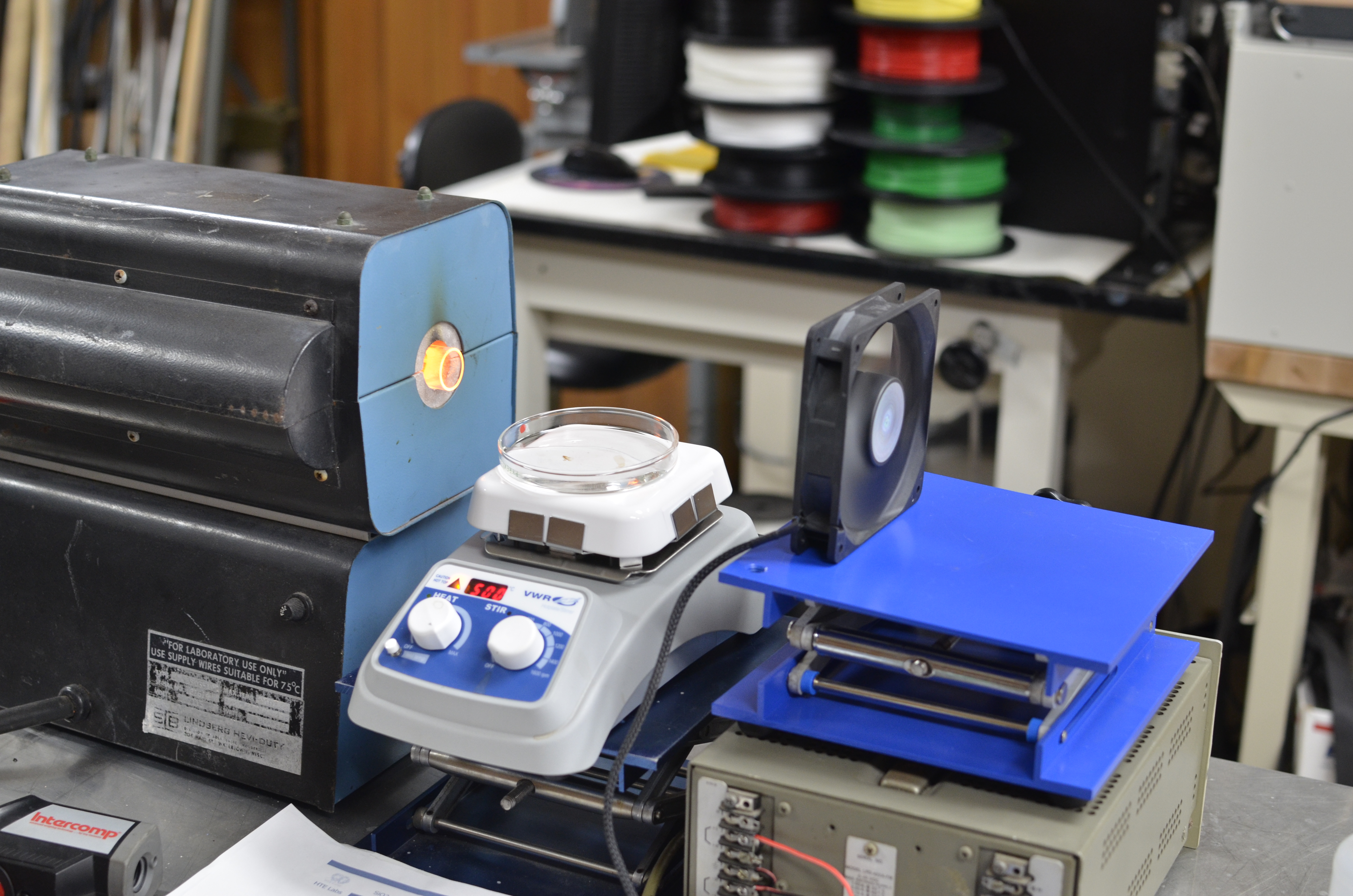
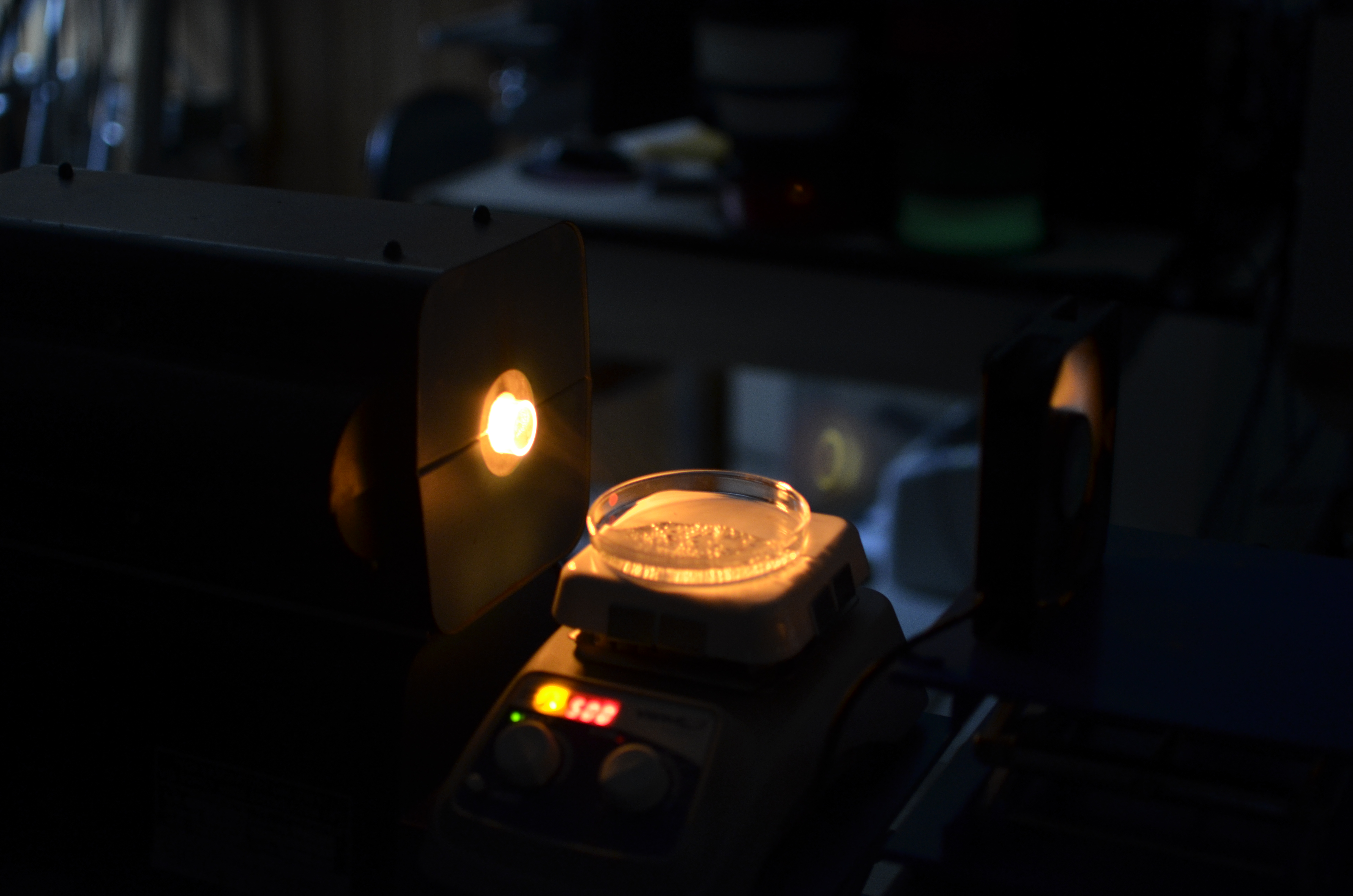
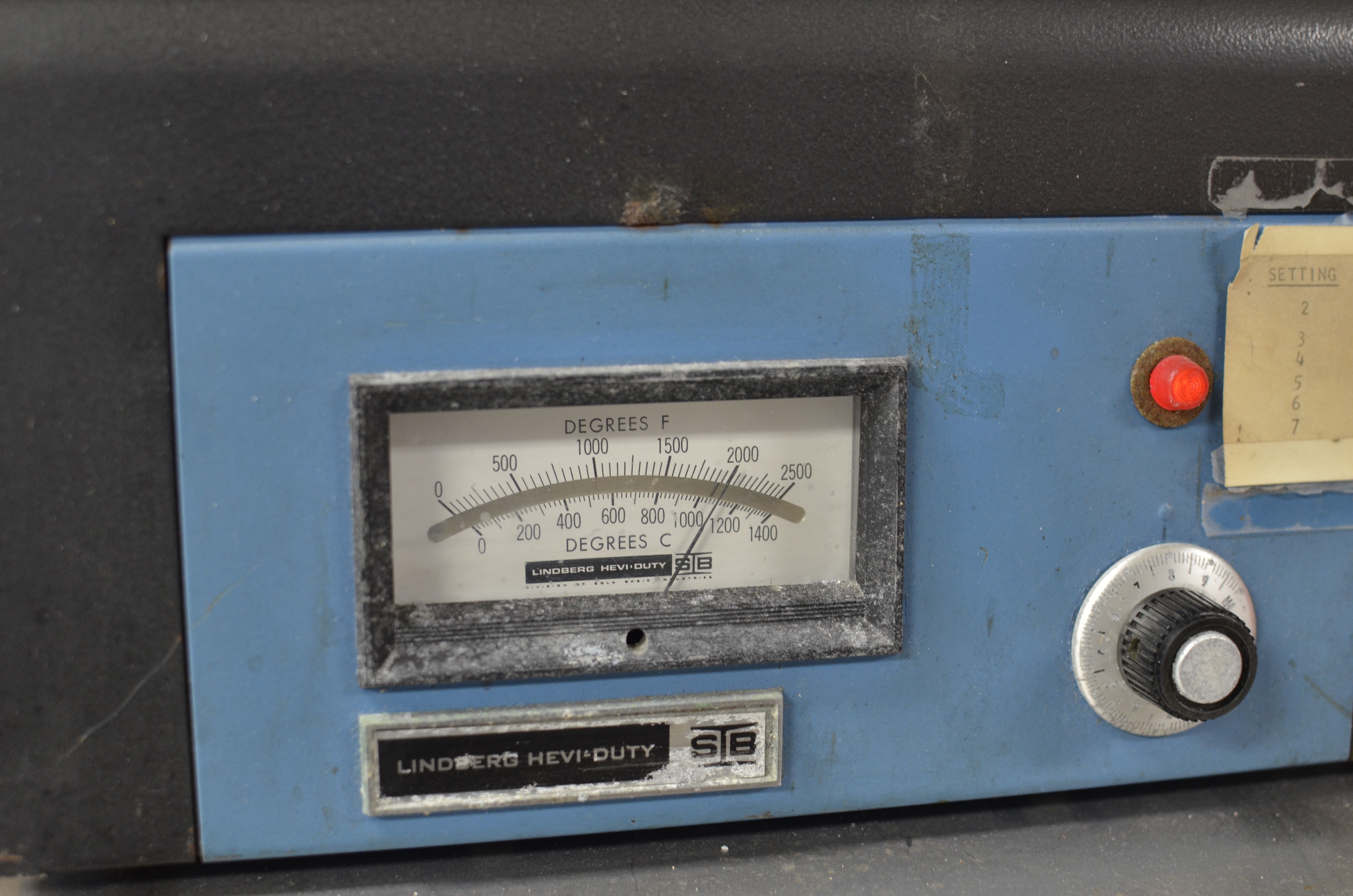
First, SiO2 is thermally grown on a test wafer using a water vapor source on a nearby hotplate to fill the furnace with steam during oxidation. The first step to ensure good resist adhesion is a dehydration bake which creates a hydrophobic wafer surface. This does not need to be done if the wafer recently came out of the furnace but if it has been in storage, then a bake of up to 700C may be necessary to restore the dehydrated surface. The next step is HMDS vapor priming:


Here, the wafer is heated to around 200C in the presence of Hexamethyldisilazane (HMDS) vapor forming a surface monolayer on the wafer that further increases resist adhesion. HMDS can also be spin coated but this often yields a far too thick layer and can lead to incomplete photoresist development.
The final steps before etch are to spin the resist and to hard bake it. Naturally, a thicker resist film allows for a longer etch time. For maximum chemical stability, the hard bake should be conducted for extended periods of time close to the resist softening point which is usually around 145C. This can make the photoresist difficult to remove, so an ultrasonic acetone bath may be necessary unless you have proper stripping chemicals. If difficulty persists, then it is likely that the top layer of resist has cross-linked and you may be unable to remove it. One may try high power Oxygen RIE followed by Piranha solution and N-Methylpyrrolidone (NMP) stripper as is used commercially to remove resists after hard ion implantation.


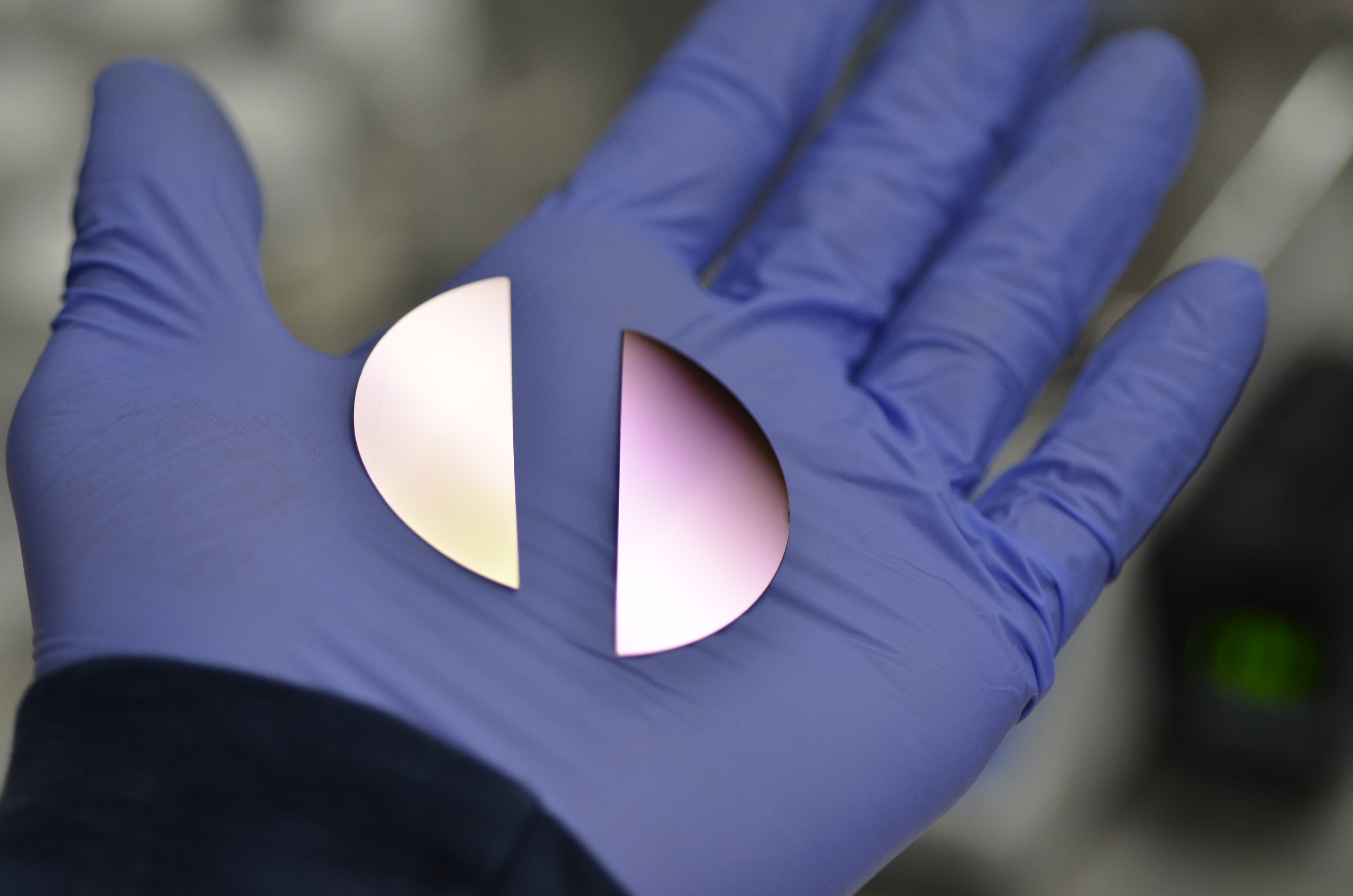
Instead of a standard HF etch, a buffered oxide etch of NH4F (Ammonium Fluoride) in HF can be used to control the etch rate and photoresist lifting. I use approximately 20-30g of 100% NH4F per 50mL of HF (stock whink rust remover) and etch time for 6000Å SiO2 is 20min at 20C. A couple drops of Triton X-100 nonionic surfactant may be added to the BOE to improve etch uniformity, wetting, and ensure consistency through a thicker resist. A good BOE recipe can be found here but assumes industrial-strength HF.


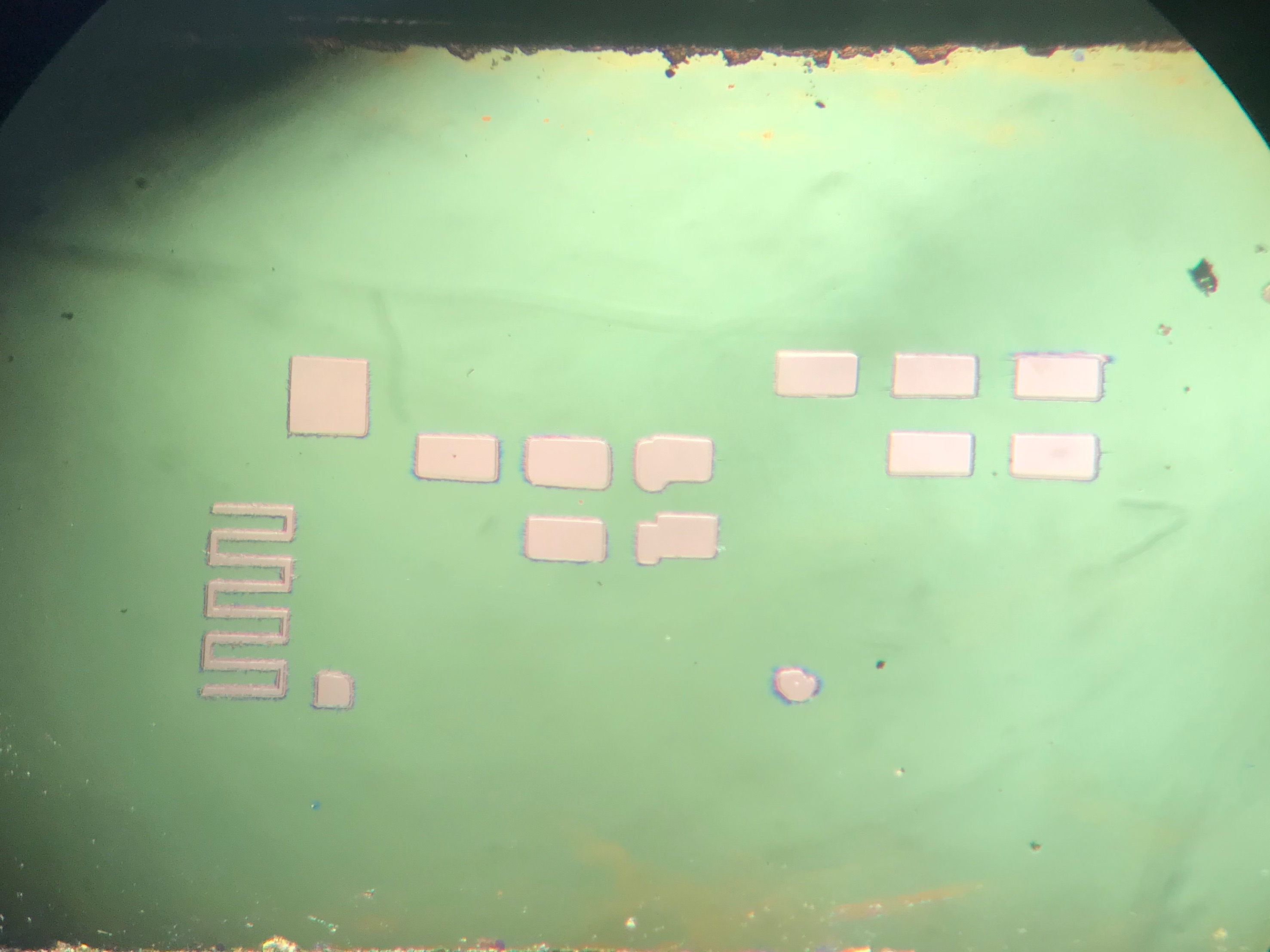


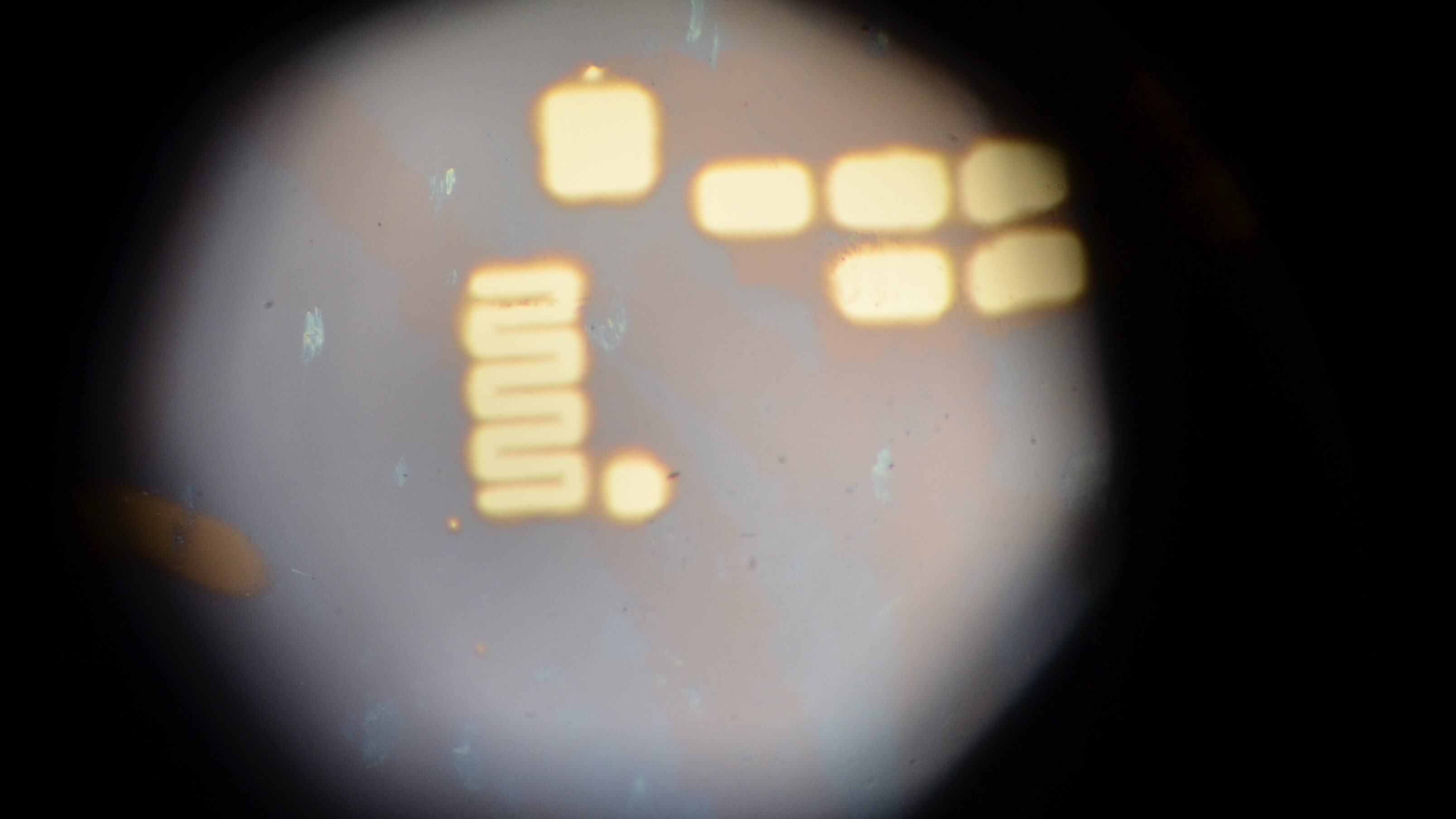
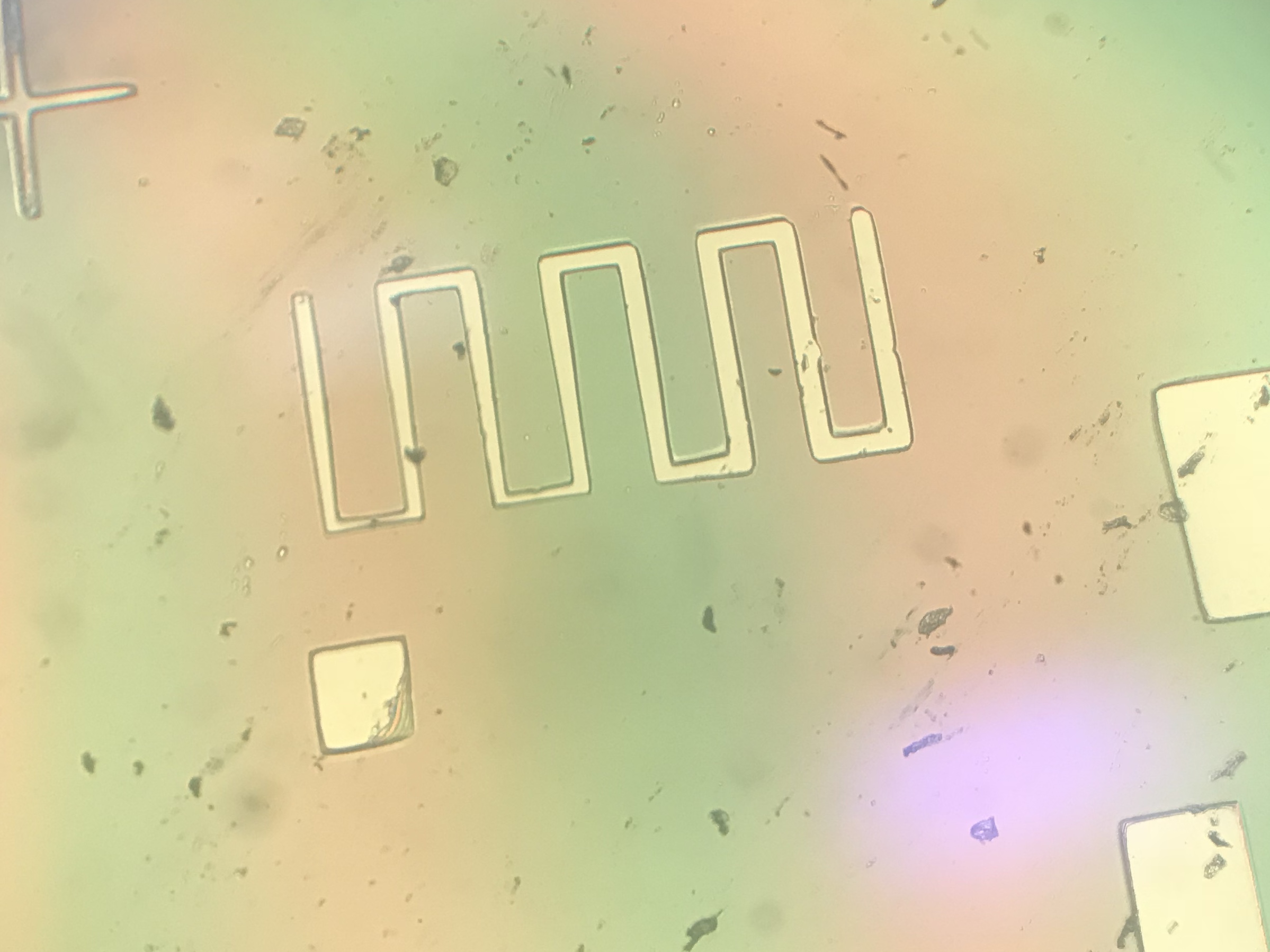
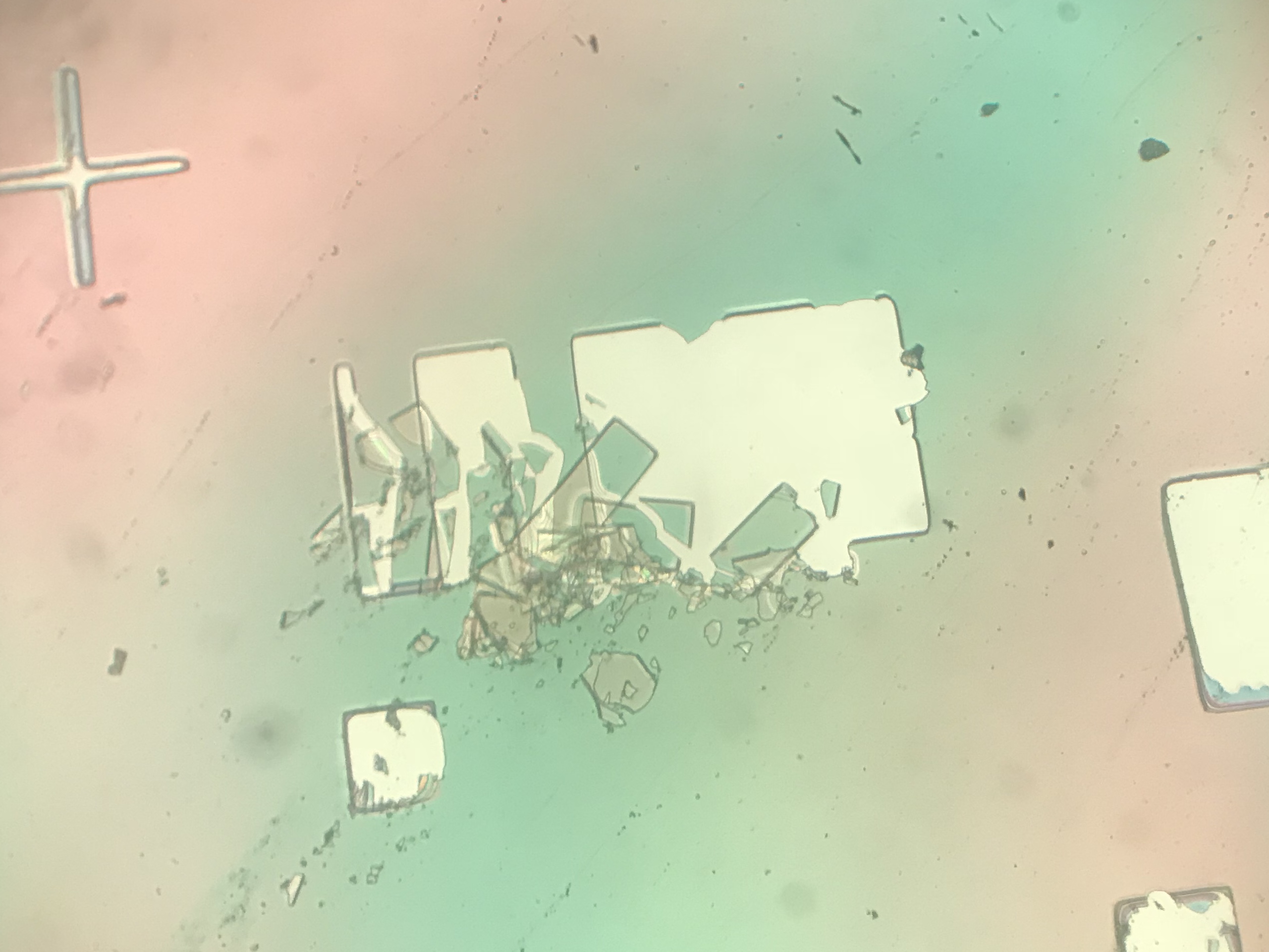
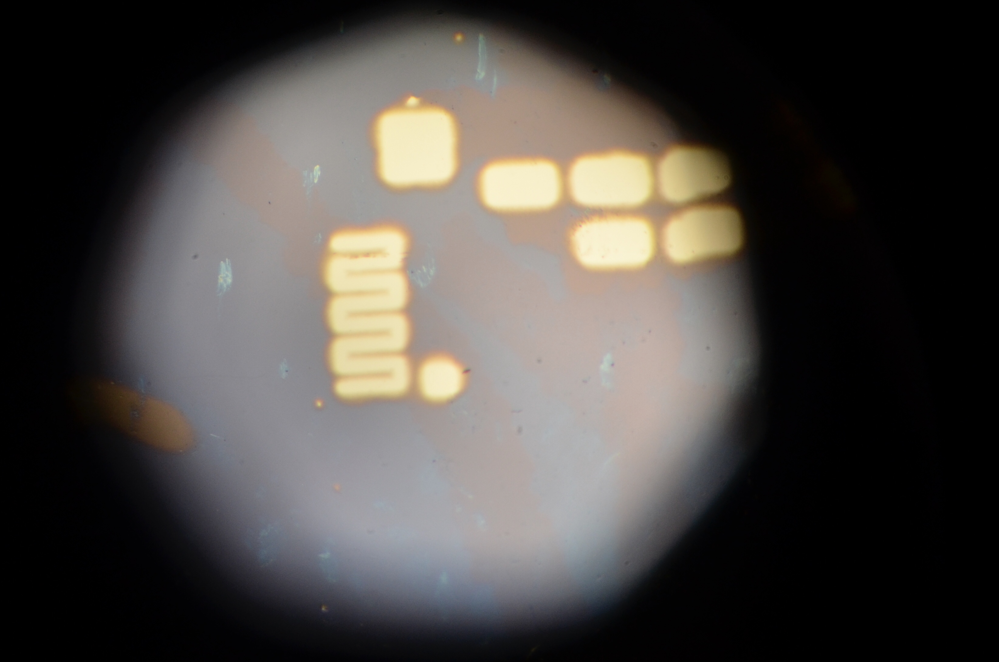
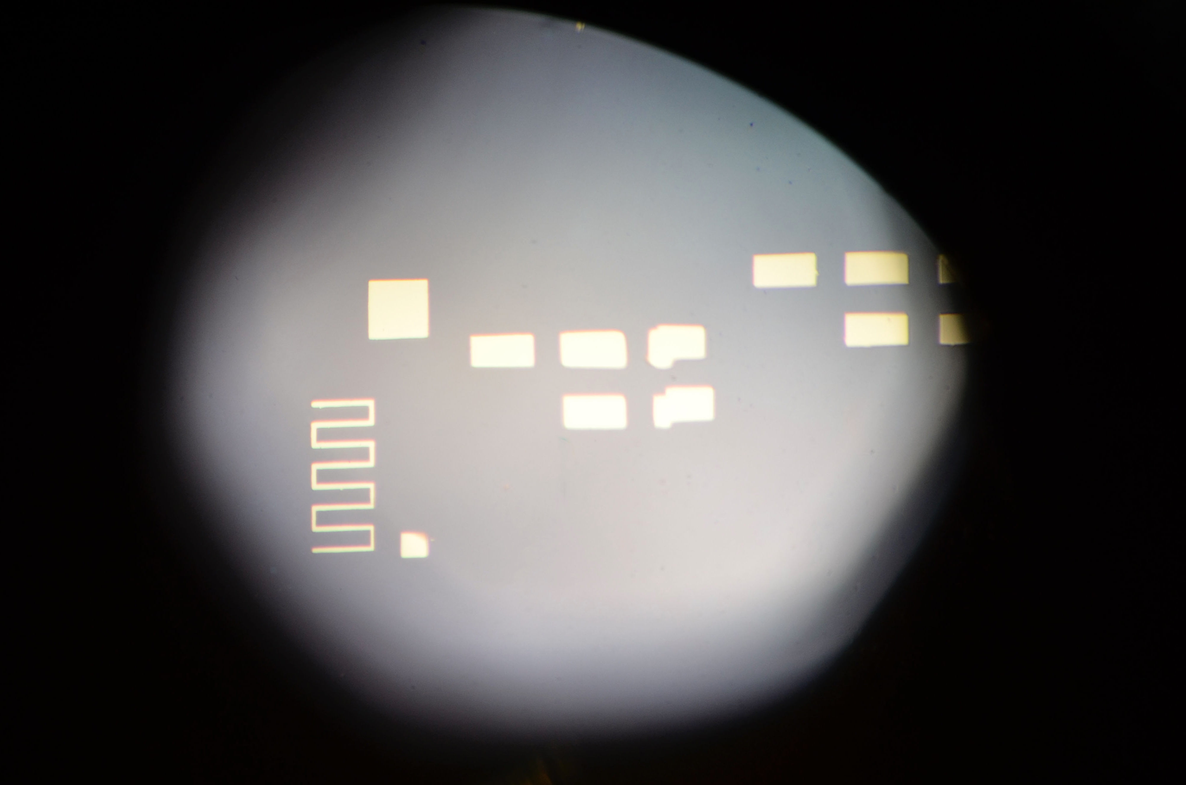
Etch trials
Have you tried different gate ox thickness for different vth? Your can really customize
Garage or not, a man certainly of unwavering will. Bravo Sam Zeloof, the disturbulence of your cognition is a negentropian lifeform.
Thank you for this very detailed and digestible walk though integrated circuit fabrication. Its great to be exposed to these processes and terminology (and photographs) to learn what challenges are involved.
Thank you for your share,it is better than school book,that is realy technology
Instead of HF, could atomic hydrogen be used? (SiO2 + Hn -> H2O + SiH4, or would the result be an ugly amorphous blob of partially reduced SiO2?)