Homemade Silicon MEMS
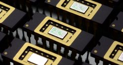
The term MEMS was first coined in the 1980s and has since brought tons of innovative/insane fabrication techniques and incredible devices. Among my favorite examples of this is the DLP technique invented by TI and a DNA nanoinjector for cells made at BYU (pictured below). Obviously, I won’t be making anything this complicated but had some decent results on my first attempts that are worth sharing and continuing to work on.

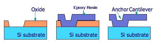
All of my MEMS devices are fabricated with chemical etching and maskless photolithogrpahy. The most basic free-standing mechanical device is the cantilever, which can be made using a sacrificial underlayer made of oxide or photoresist (SiO2 in my case) and a harder upper layer (SU-8 epoxy resist in my case) which remains when the sacrificial layer is removed with chemical etching (HF for SiO2). These can be made into oscillators, nano balances, any many other useful instruments.
There are many variables here to optimize, so it is best to run many experiments at once.


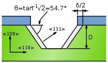
The next MEMS technique to demonstrate is bulk Silicon Micromachining which leverages the high level of order in a monocrystalline Silicon wafers to make controlled and often self-terminating etches. On a standard <100> orientation wafer, a solution of KOH (KOH pellets from amazon/ebay dissolved in water) can anisotropically etch Silicon to expose the <111> crystal face at at an angle of 54.7º from the wafer surface.
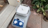
The setup for this is quite simple, 60% KOH solution with a dash of isopropyl alcohol is brought to 80°C in a hotplate with stirring and etches about 90um in 1hr, or about one-third the thickness of a Silicon wafer. Nature’s fume hood is used for this experiment.
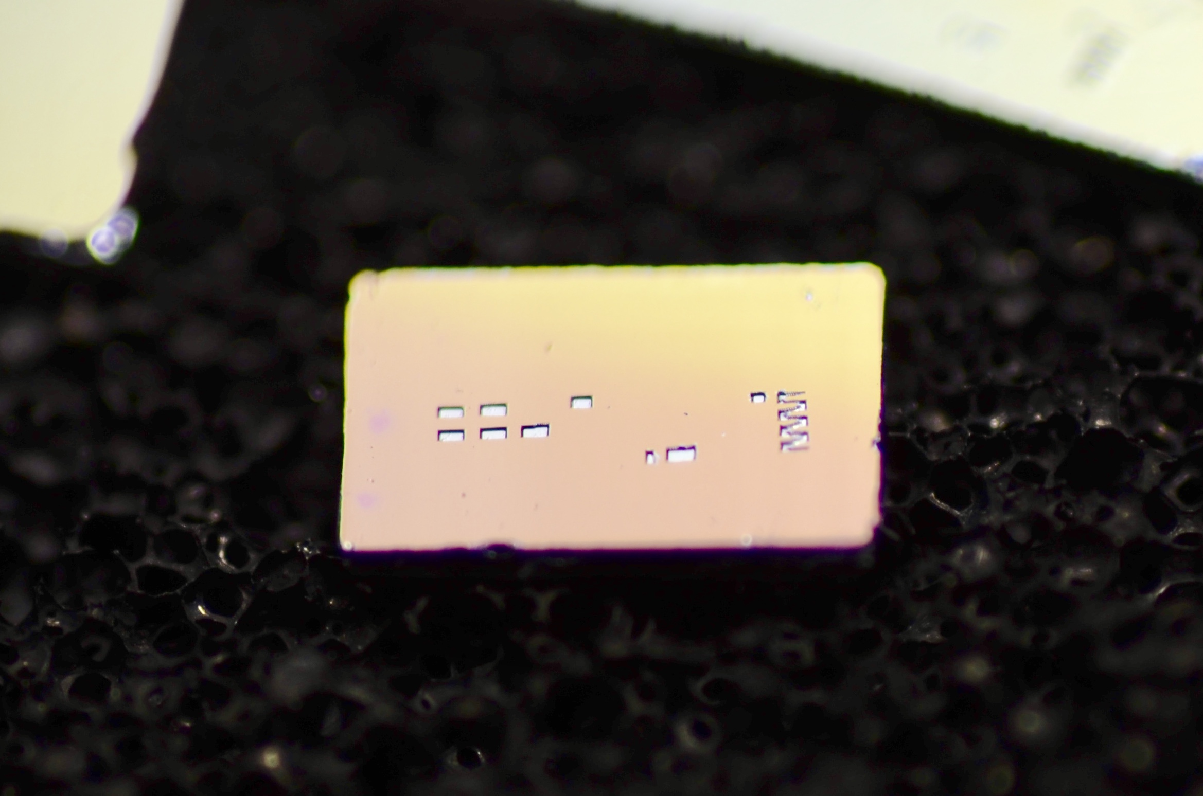
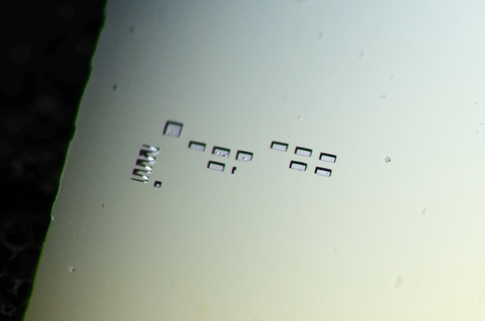
A top layer of SiO2 is used as a hard mask to etch the underlaying Silicon. Before KOH etching, the SiO2 is thermally grown and patterned in a standard process by maskless photolithography and HF etching. The active layer mask for my Z1 amplifier chip was used here as a quick and convenient anisotropic etch test. Wafers are then inspected under SEM.
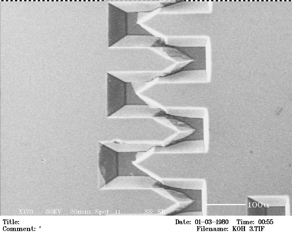


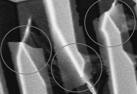
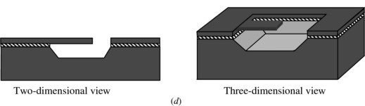
Suspended cantilever-like structures can also be made here. The first KOH etching attempt shows some undercutting, but in the future stirring conditions will be optimized to provide more undercutting. The circled areas in the high-tilt angle SEM image below show 500nm thick SiO2 overhanging 90um of airgap above the Silicon surface.
Just wanted to drop a line and say that what you’re doing is amazing and you’re probably one of the few people around the world who have a setup like that at home. Best of luck to you! Thank you for putting up this website for other to see the process and everything that goes with it.
Parabéns
My eyes sparkled. There are so many researches, experiments and spent a lot of time in the lab. I wish i would have several $M s to support you; but i don’t have any for now. But you did a nice and remarkable job. Best wishes for you from much older earth location. Good luck Sam…
As a fab process engineer who have worked with the real process tools I am seriously impressed with your ingenuity to do this fabrication as a garage project.
I am especially impressed with the use of a DLP HT projector as a mask less exposure tool and the fact you have stepping and alignment with submicron resolution!
Maybe one of the next tools you want to make is a plasma tool, you could make a parallel plate plasma etcher, a resist stripper, possibly even a small ICP etch tool… I think these are definitely within your capabilities – There are A/C work vacuum pumps for a ~$200 that will pull down to 2.2mtorr base, with reasonable flow that should work for these. If you can do this, you could maybe do CVD & sputter too!
BTW do you have a particle controlled area? If not checkout soft walled clean rooms as a way to get inexpensive clean room space.