E-beam Lithography

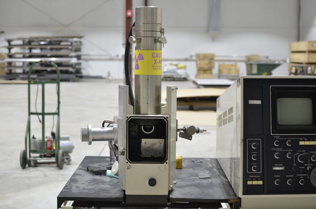
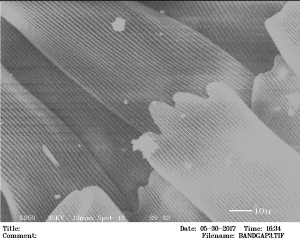
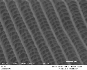
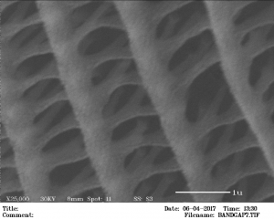
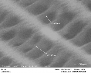
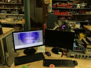
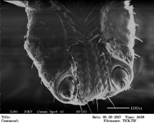
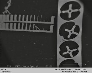
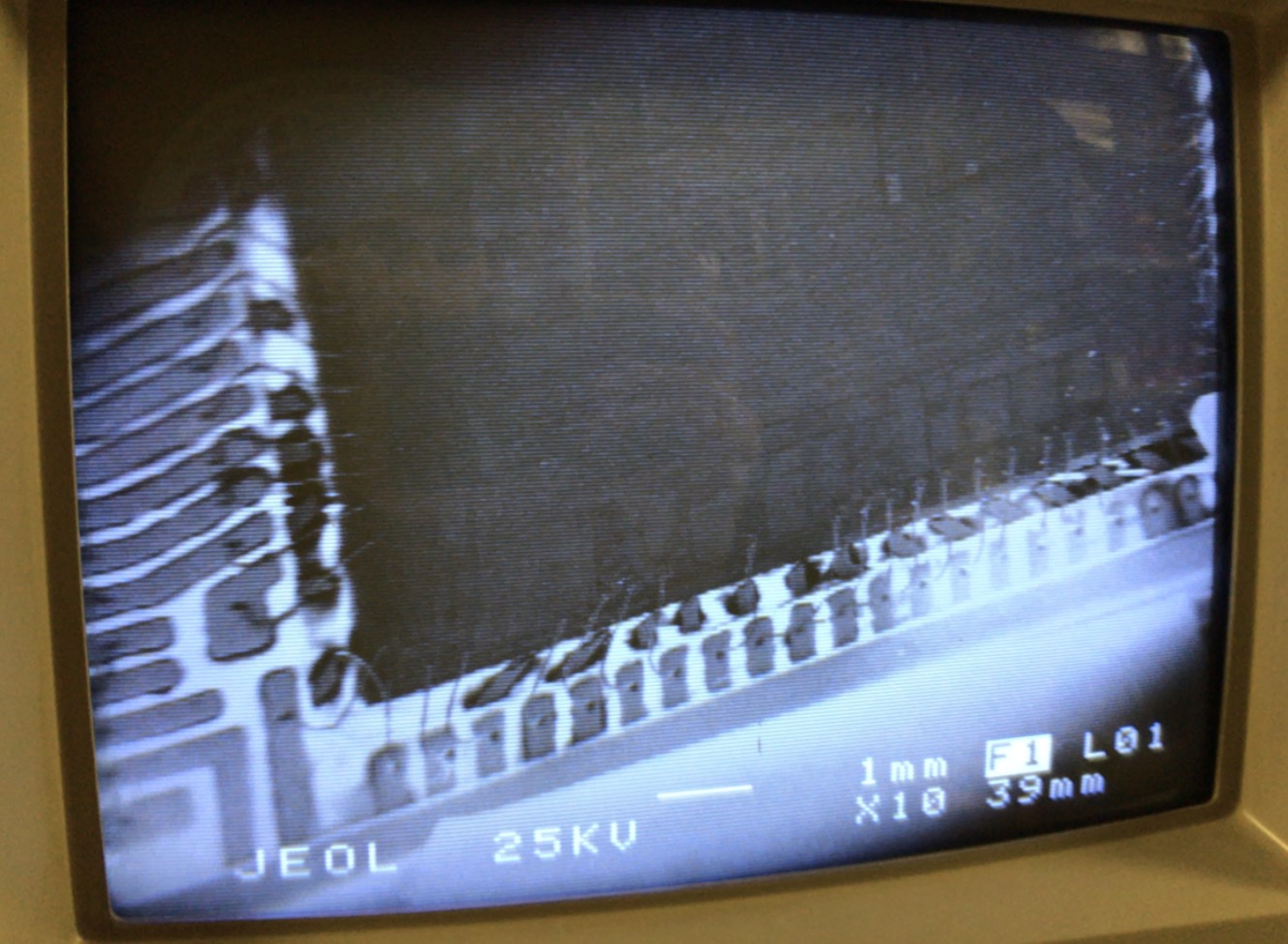
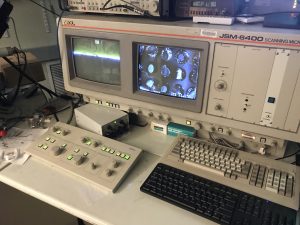
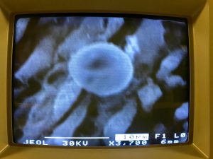
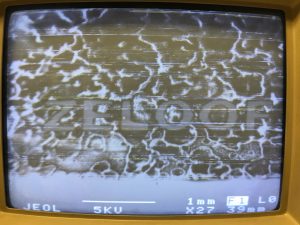
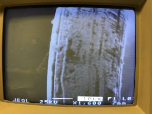
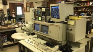
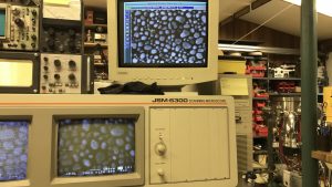
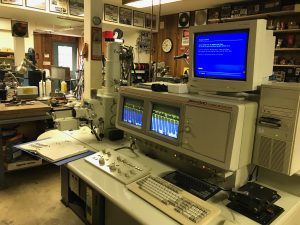
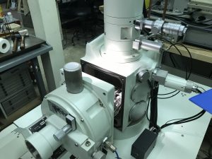
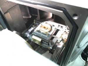
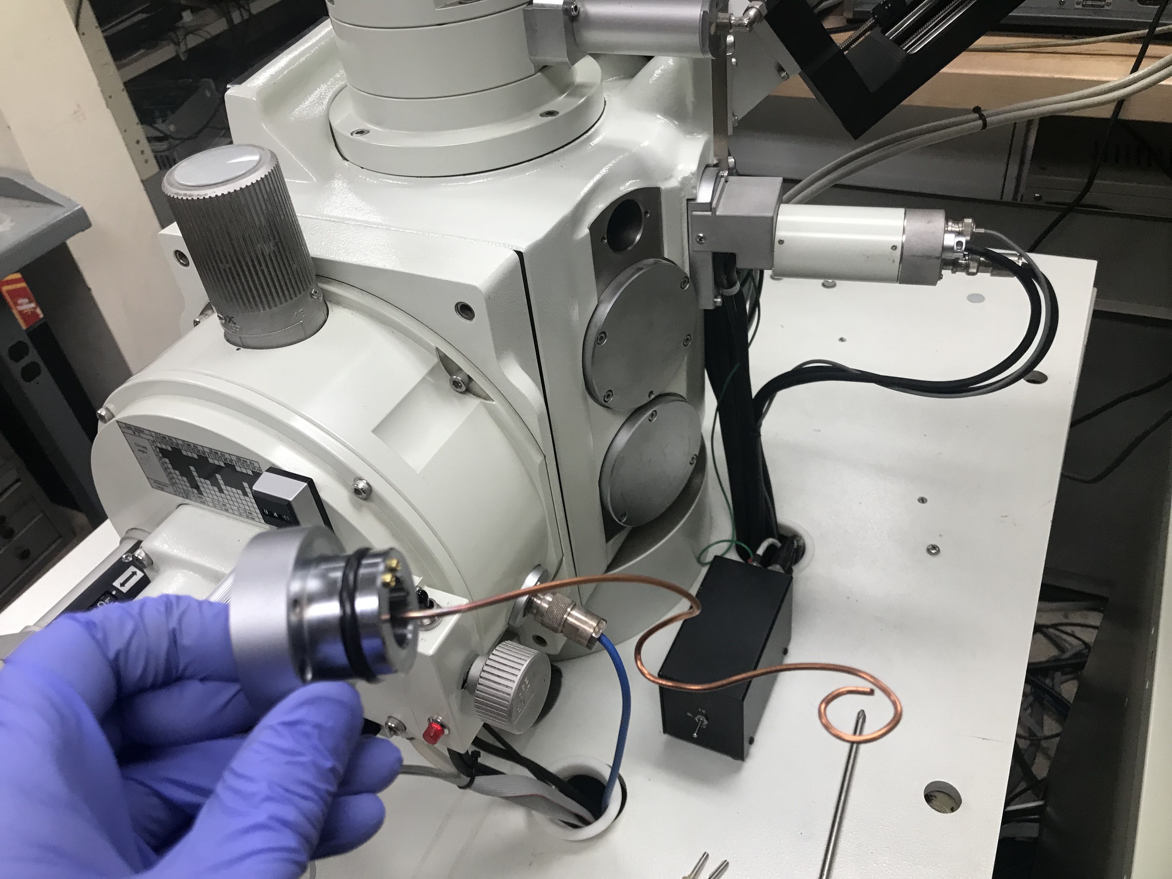
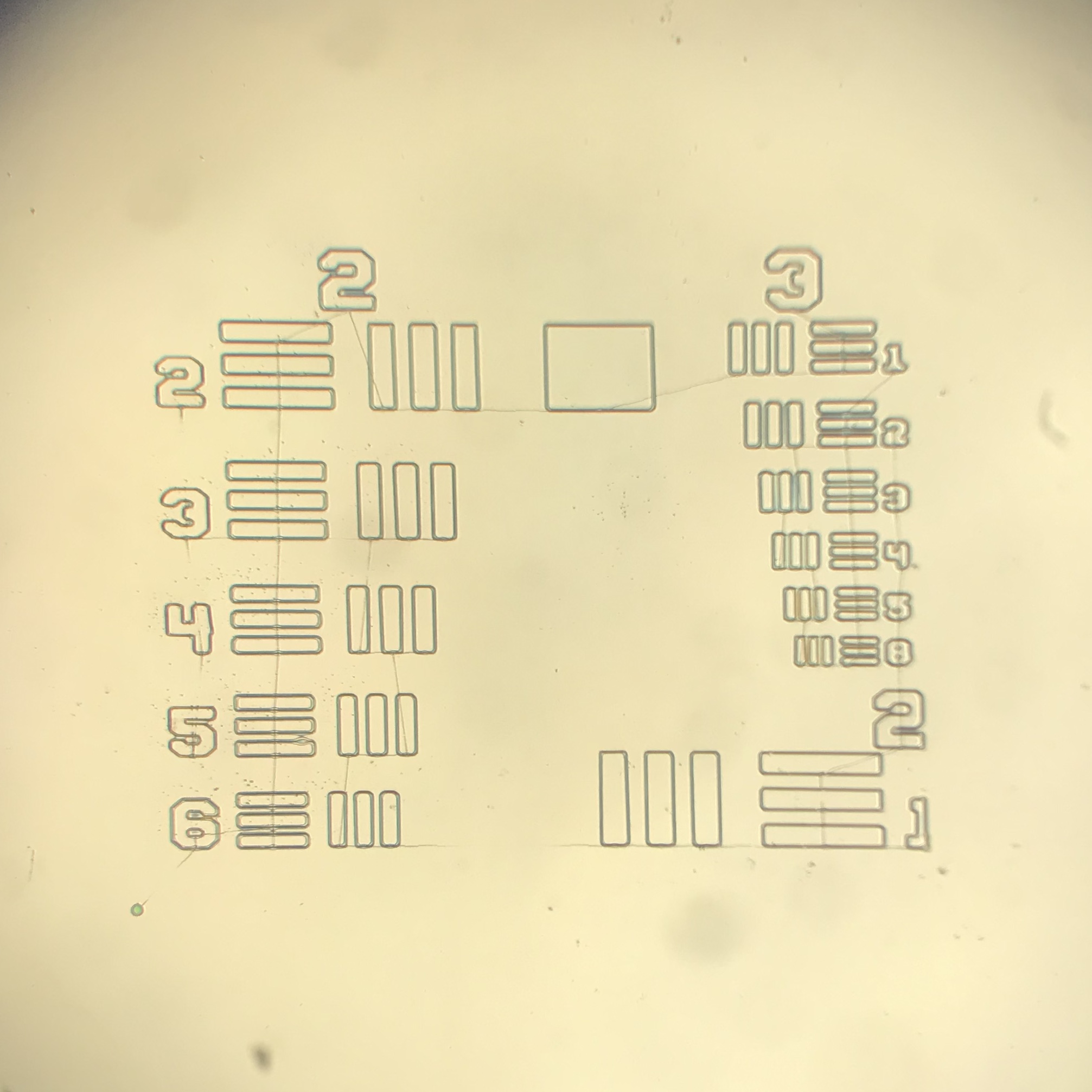
I modified my JEOL scanning electron microscope to not only image tiny things, but make tiny things too.

DSC_8877

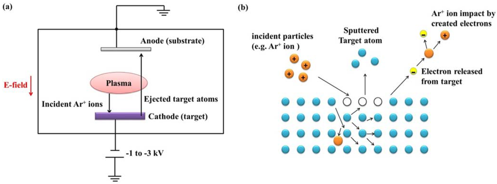
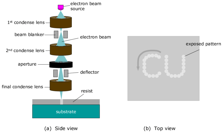
This technique is called Electron Beam Lithography. Normally, a SEM works by scanning a beam of electrons over the sample and detecting secondary electrons. In this case, I built a PC scan controller that “drives” the electron beam around and draws the image onto the sample which is coated with electron-sensitive resist.

Schematic-illustration-of-electron-beam-lithography-Electron-beam-is-focused-on-a-resist
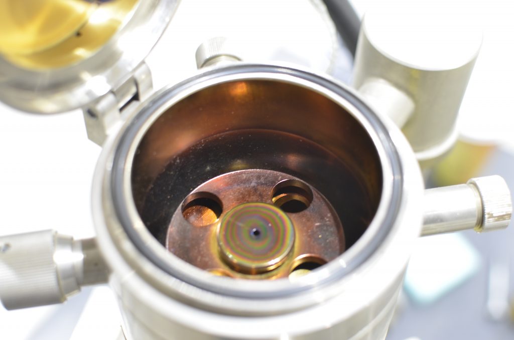
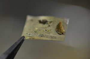
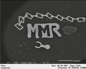
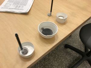
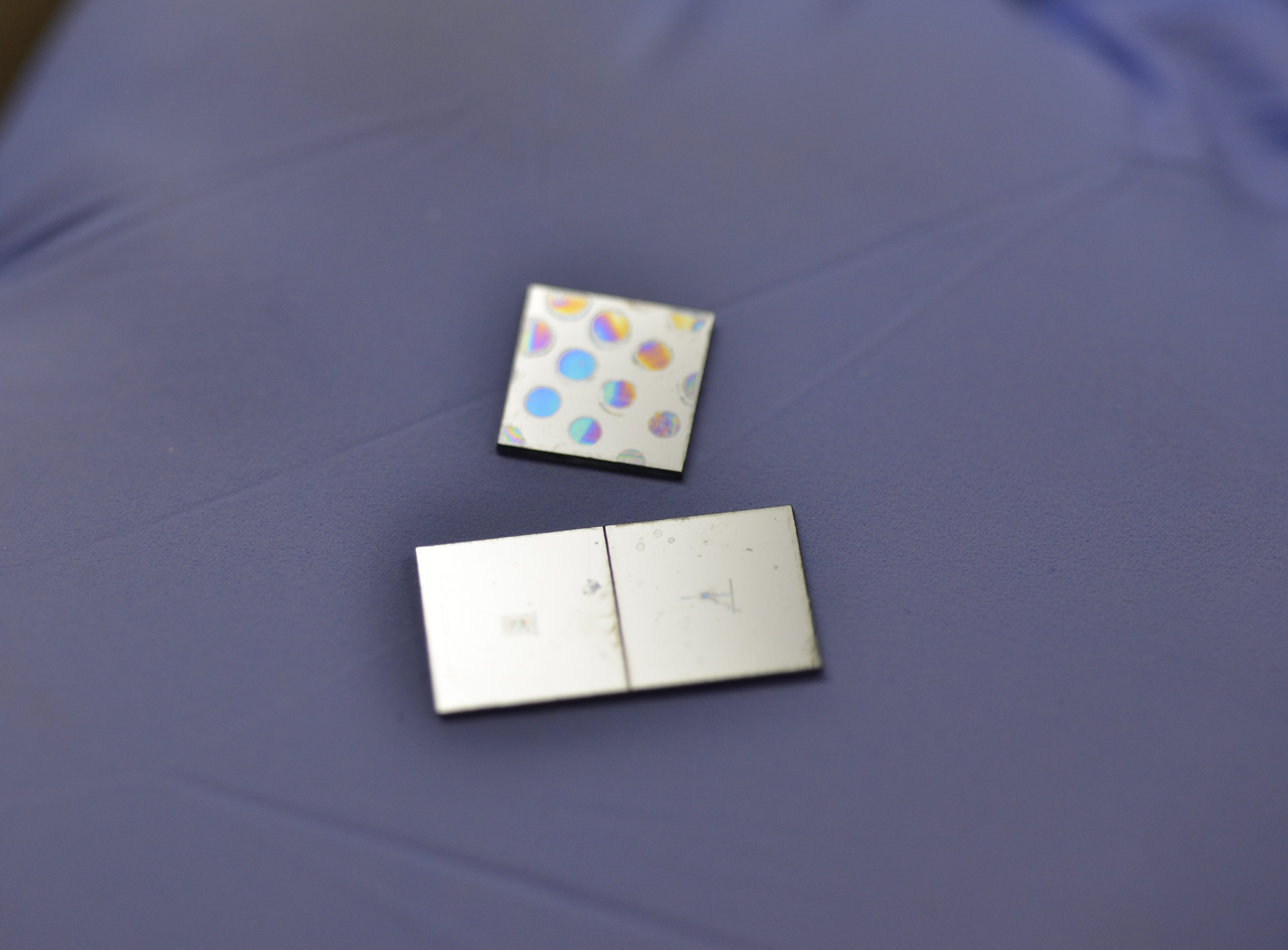
For resist, I used SU-8 although PMMA (Acrylic) dissolved in solvent will work as well.

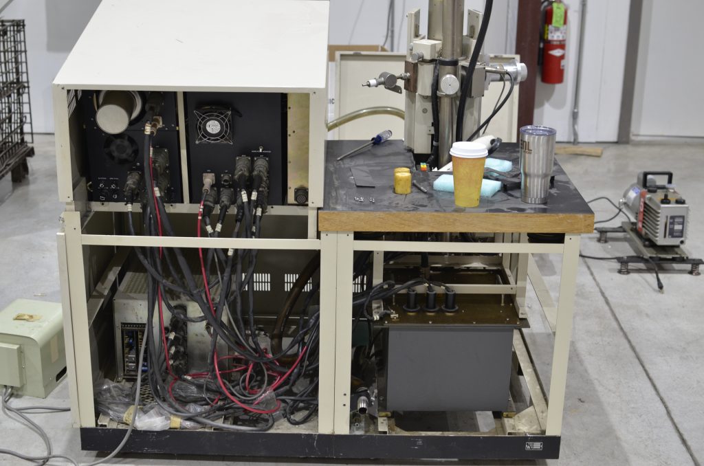
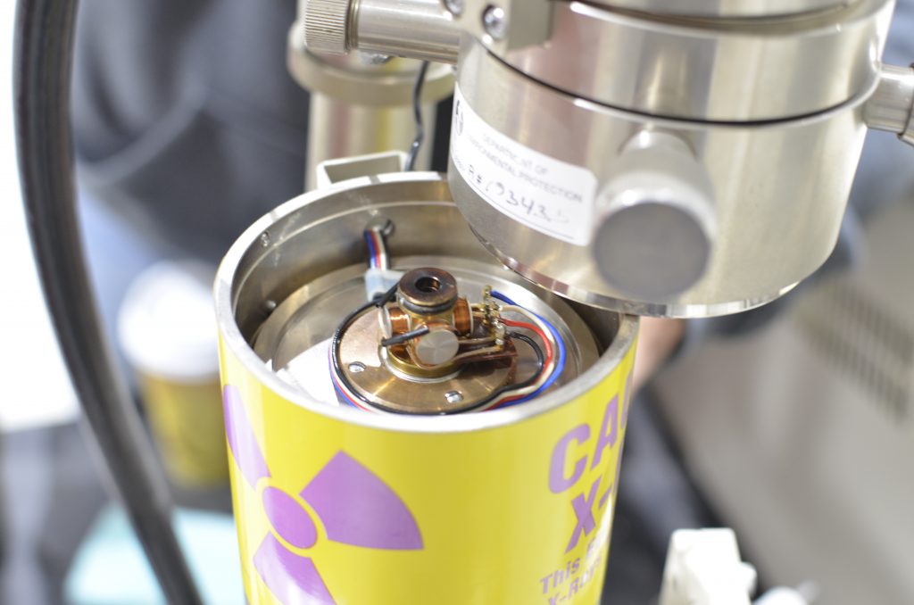
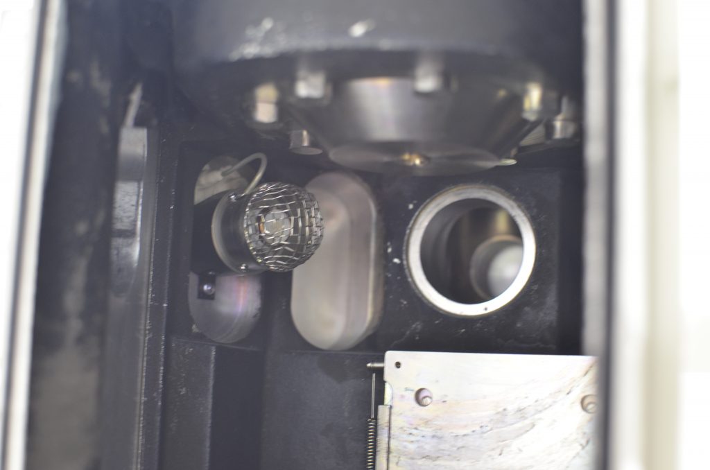
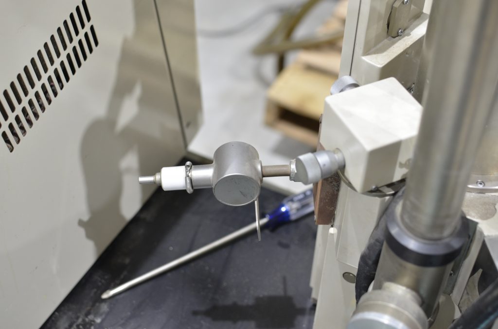
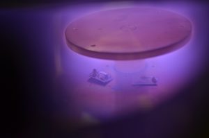
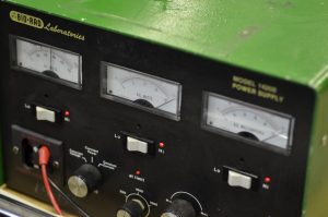
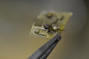
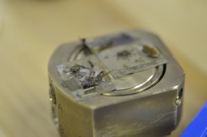
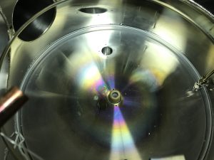
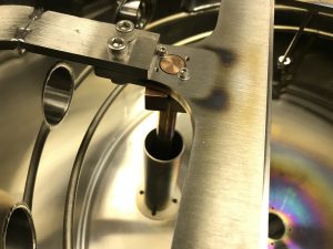
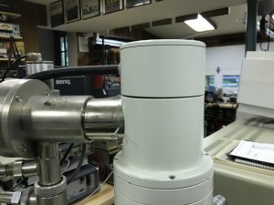
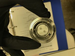
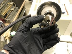
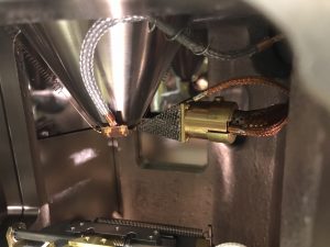
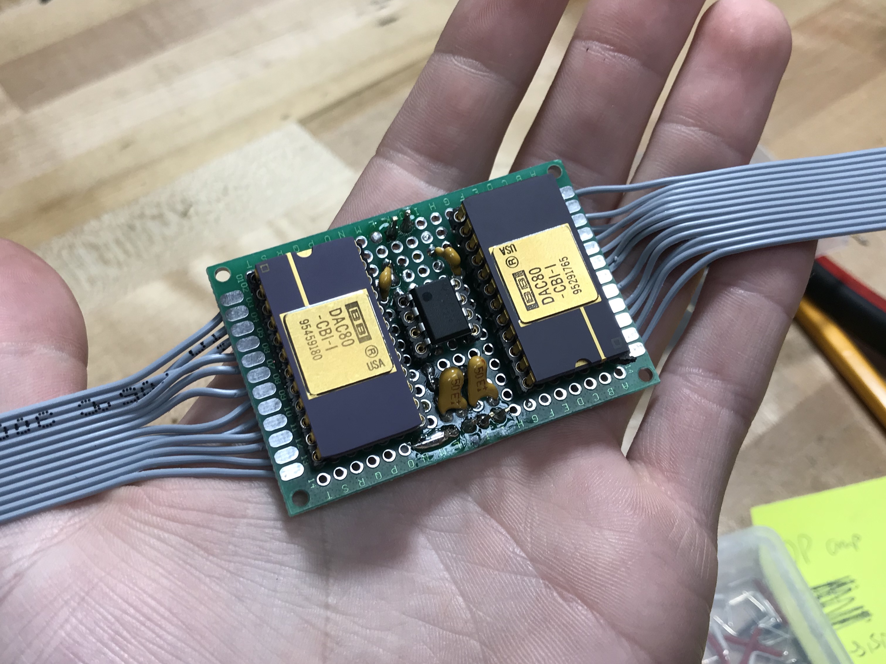
The scan controller uses dual 12 bit DACs. They had current outputs so a transimpedance amplifier creates +/-10v proportional to that current to drive the microscope’s external XY inputs. The controller also contains an Arduino and Altera CPLD. To turn the beam off when needed, a high voltage is generated (+2kv) and applied to a “beam blanker” inside the microscope.

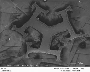
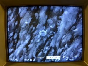
I learned that the 12 bit DACs do not nearly have enough resolution, so I will be looking at upgrading to at least 18 bits hopefully. Also, the geometry of the beam blanker is not correct to create a high electric field in its center, so the beam is only partially de-focused and never fully “turns off”.


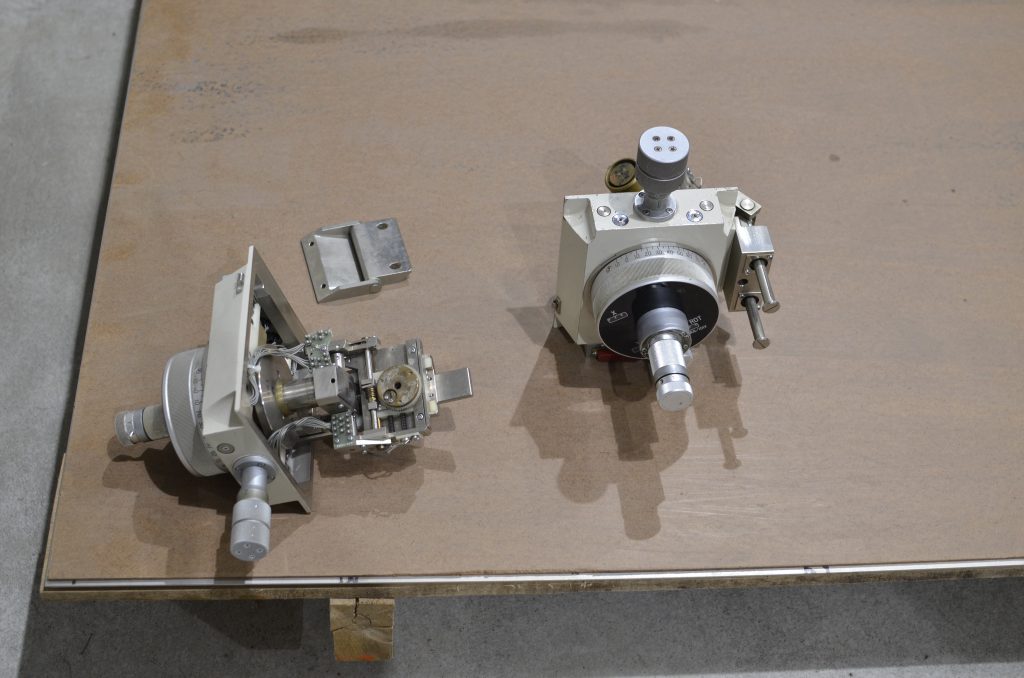
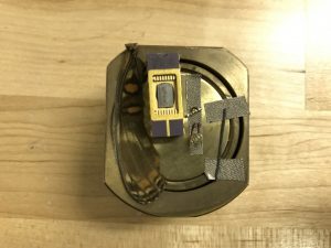
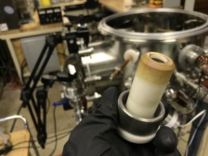
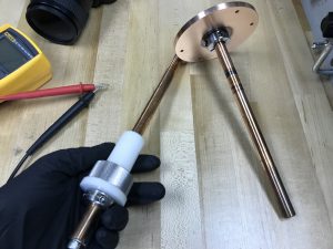
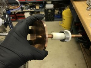
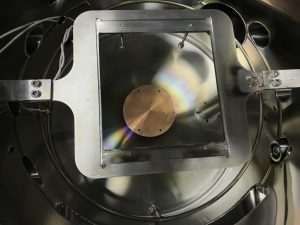
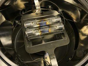
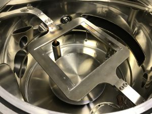
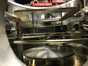
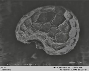
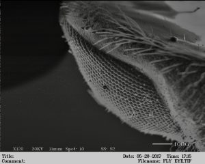
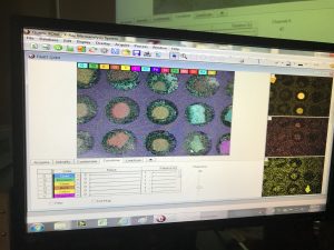
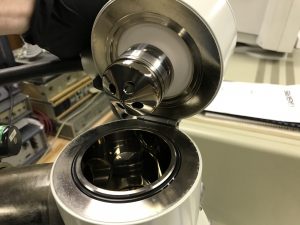
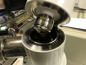
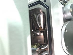
Update (2020): New photos with improved beam blanker –

Silicon Drift Detector Energy Dispersive Spectroscopy (SDD EDS/EDX) Setup

Instillation and setup of a Silicon Drift Detector EDS system. A SDD is a modern detector for Energy-dispersive X-ray spectroscopy that mounts onto an Electron Microscope and allows the user to analyze the composition of a sample. When electrons from the SEM hit the sample, it emits secondary electrons (along with many other particles and energies) which are used by the SEM to produce the image you see on screen and X-rays which are detected by the SDD to produce EDS information. The X-rays have a specific energy which is characteristic of the material and equal to the energy difference between excited and ground state electron orbitals in the atom.

The SDD (30mm2 in my case) quantizes the energies of impinging X-rays and amplifies them to be read by a computer. As compared to traditional Si(Li) detectors, SDDs are faster, have higher resolution, and do not require Liquid Nitrogen cooling.

The detector is mounted to the chamber at a 35° angle which makes it most convenient for use at a WD of 25mm. When using the SEM at lower working distances, the SDD probe is retracted out of the chamber as to avoid collision with the sample stage. The detector is chilled to -30°C with Peltier modules.

The detector has a built in preamplifier. The output is fed to a pulse processor containing an FPGA which connects to a laptop via ethernet.With the SDD, EDS spectra can be acquired in less than a few minutes at high beam currents.

(Click on image to enlarge)

Thanks to Pulsetor LLC, Rick Mott, Jeff Thompson, David Bono, and John Guerard for their extreme generosity and help with the detector.

Photonic Nanostructes in Butterfly Wings – SEM Analysis

Nano-scale features on butterfly wing scales interact with specific wavelengths of visible light (photonic bandgap material) to produce bright colors as observed by the human eye. This structure, for example, removes certain wavelengths from the white light that hits it (mainly blue, 472nm) so that the color, when observed by the human eye, appears orange.

SEM Sample Preparation – DC Sputtering

Thin films of copper were prepared on non-conductive samples to be observed under the Electron Microscope. This process is called DC Diode Sputtering and took place at just below 100mTorr and 2000v @ 150watts.

materials-07-06377-g004-1024

This same setup can be used at lower powers to plasma clean or etch the top layer surface of the sample for better images under the SEM. Oxygen (and sometimes a small amount of Nitrogen) is usually a much more effective gas for this cleaning than Argon and leads to less unwanted sputtering as well.

Sputtering system v2 was made to support DC and RF sputtering so I can make dielectric coatings as well and it supports larger target and substrate samples. An insulator will be constructed to mount the target holder to the main chamber walls so that RF can be used more effectively.

(Click on image to enlarge)

SEM Demo

Garage Electron Microscopy – First Images

A huge thanks to David Bono from the DMSE UGTL lab at MIT for training me in basic SEM operation during a recent college visit on MIT’s JEOL JSM-6400, which is very similar to my JSM-6300. Because of David Bono and Colin Marcus’s generosity I was able to get my SEM up and running.

thumb