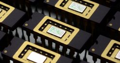
Update 8/26/17: Developing Patterning Process for Homemade Microelectronics
The general idea is to use a modified presentation projector and reduction optics to transfer an image to the photoresist on a wafer without the use of expensive masks. Below are descriptions of the 4 iterations of my photolithography setups:
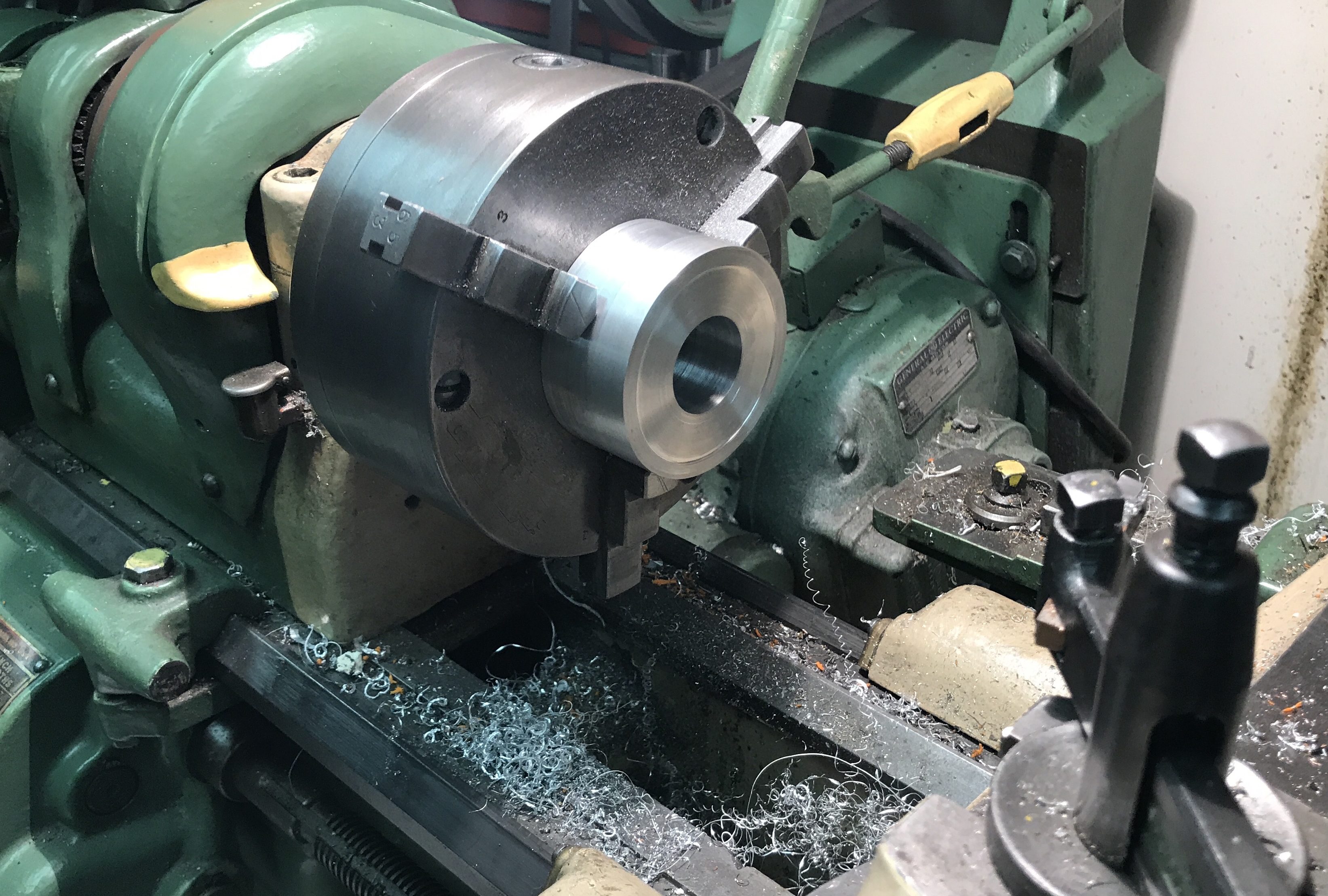
Mark IV:
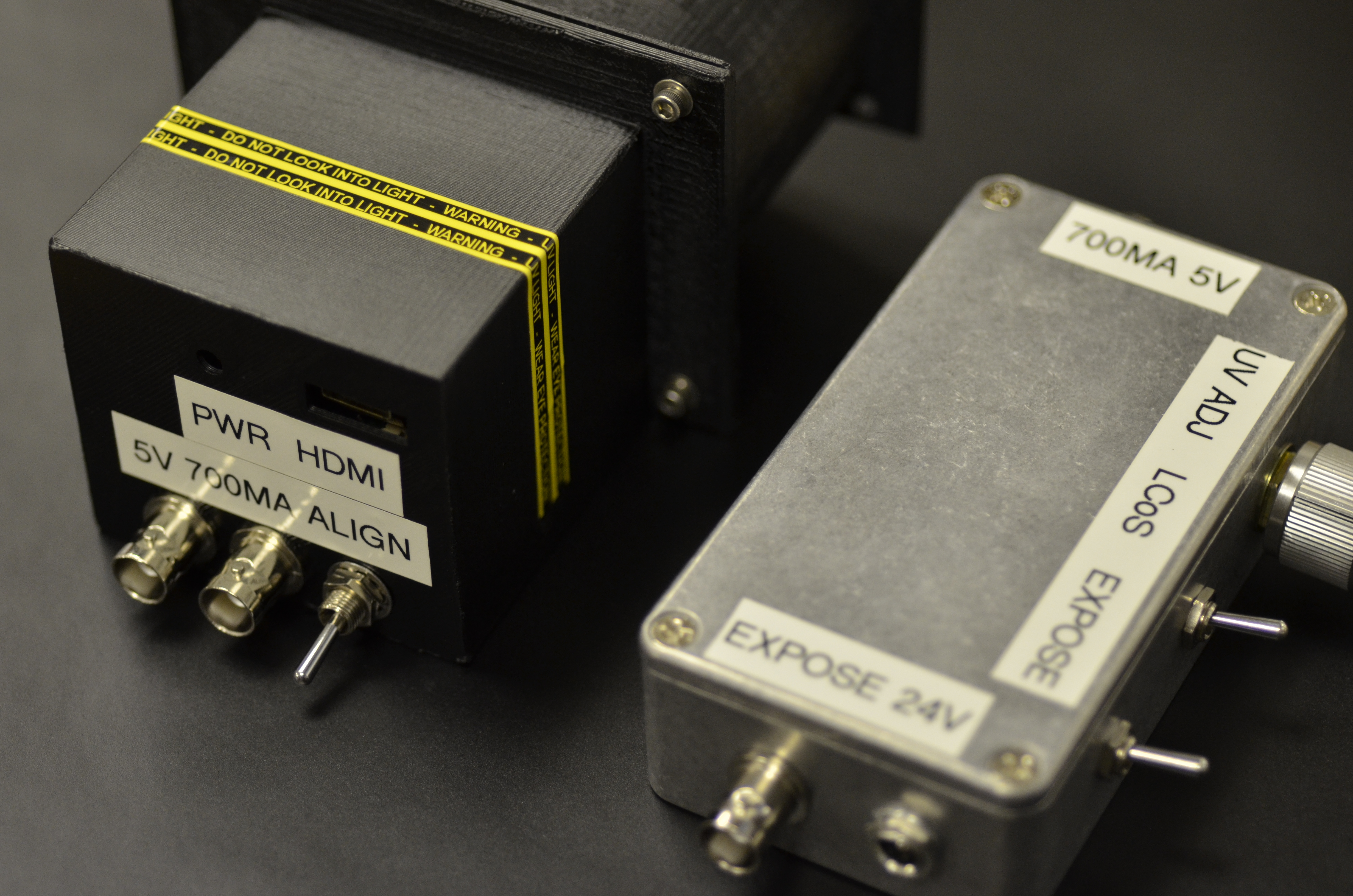
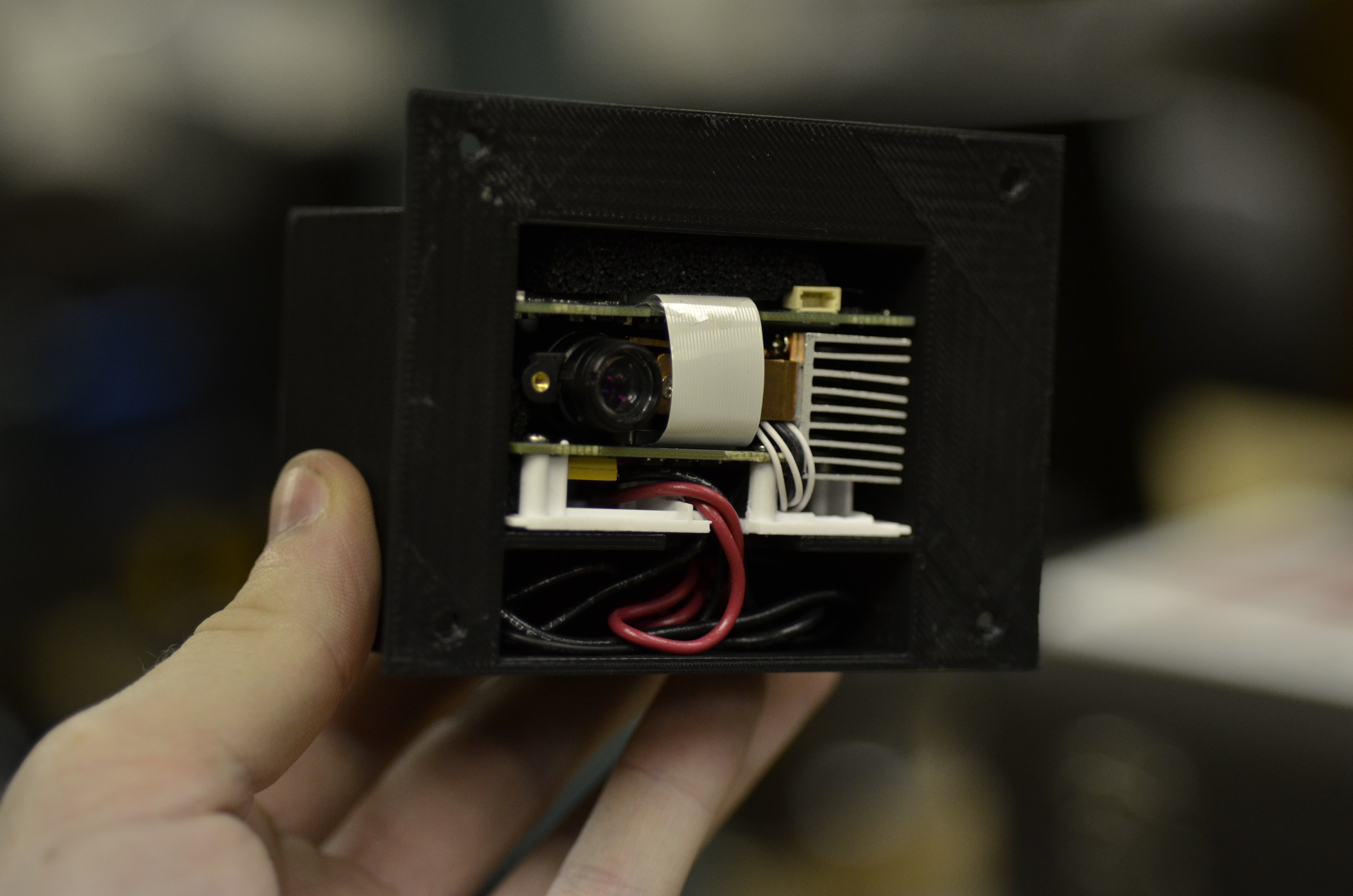
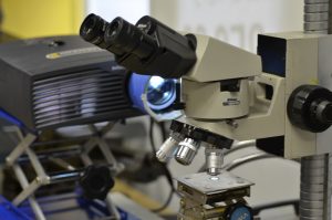
Automated DLP submicron stepper for 2″ (50mm) wafers with LabView control, computer alignment, and wafer vacuum chuck

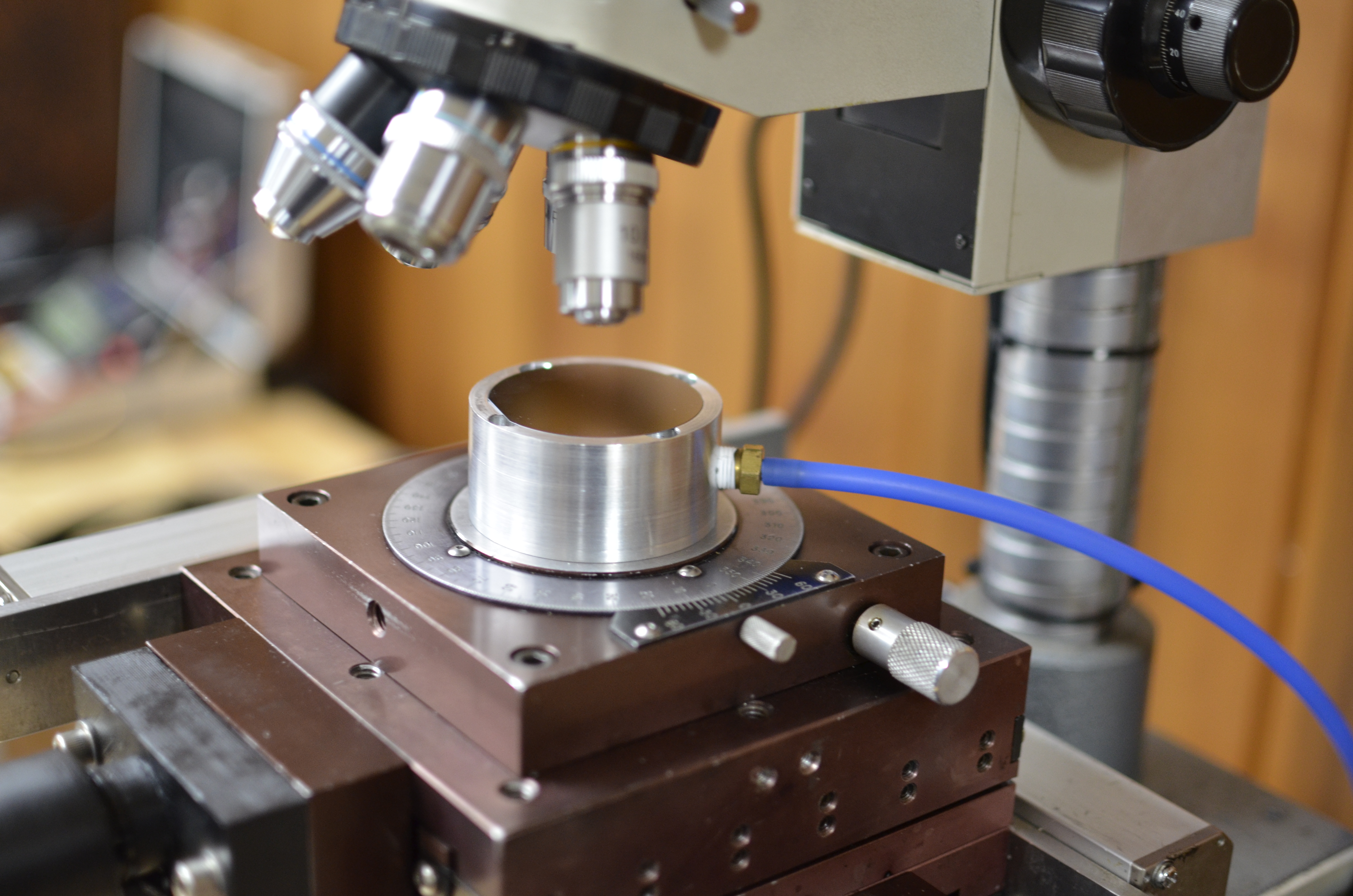


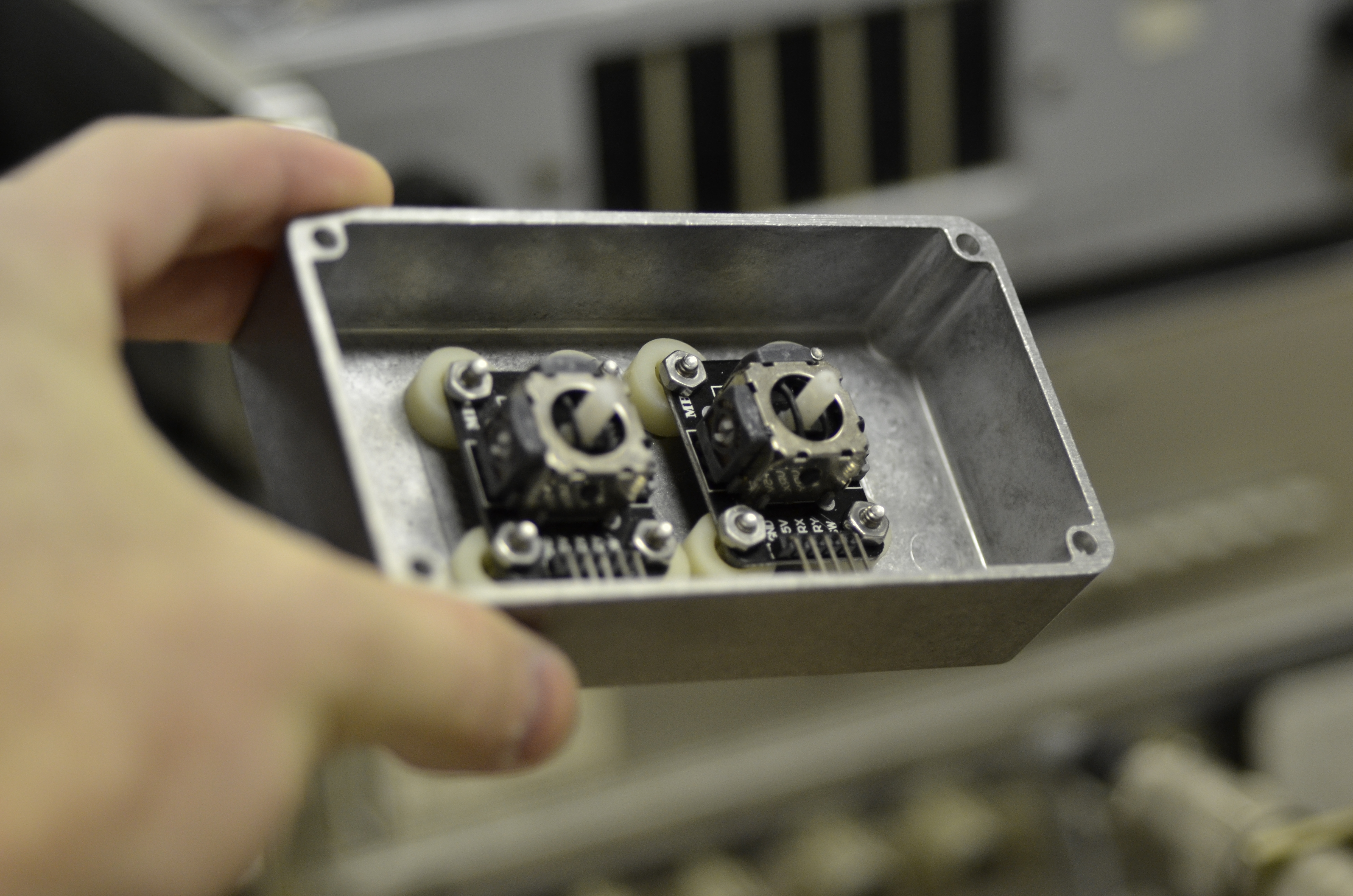
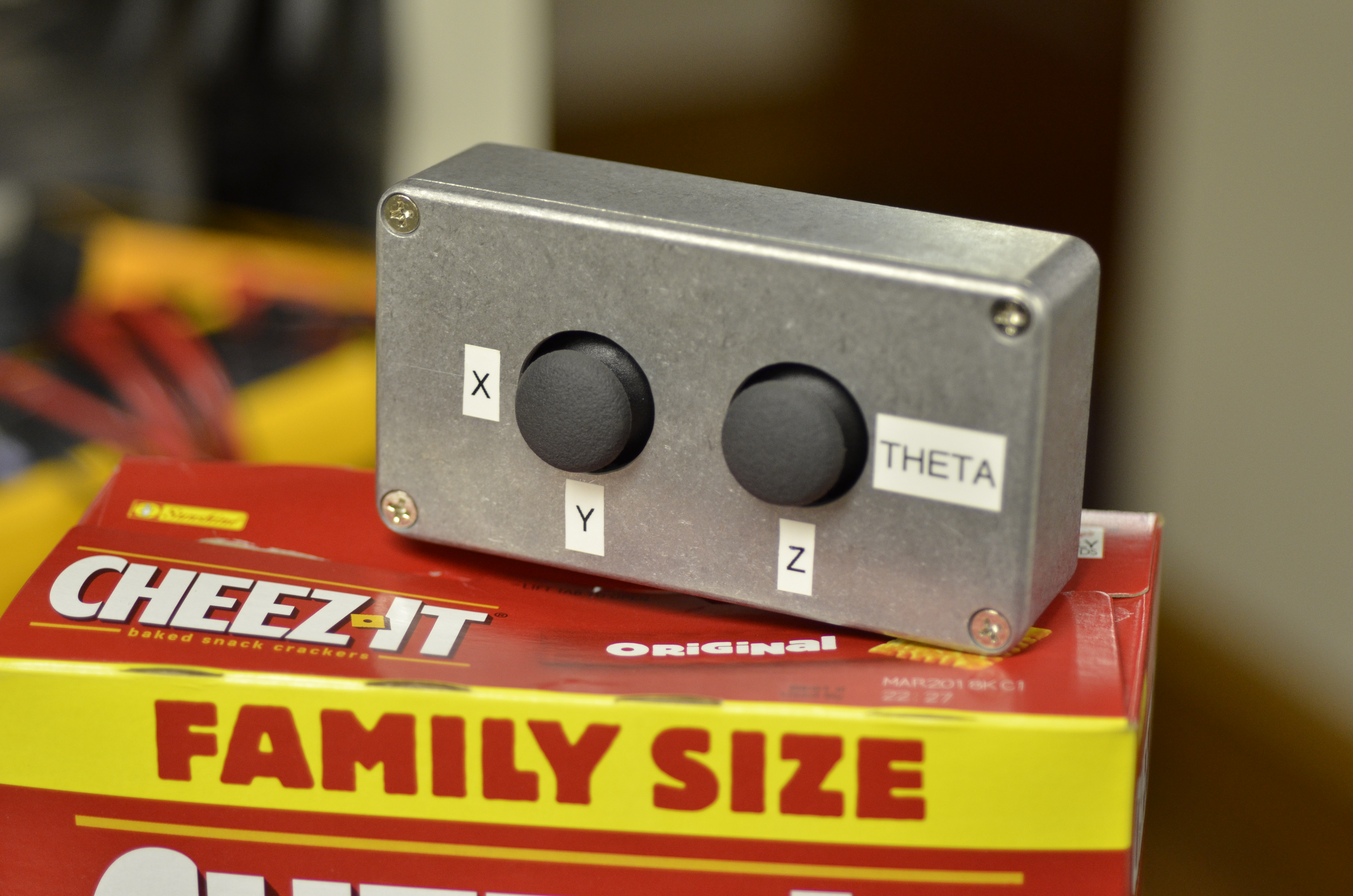


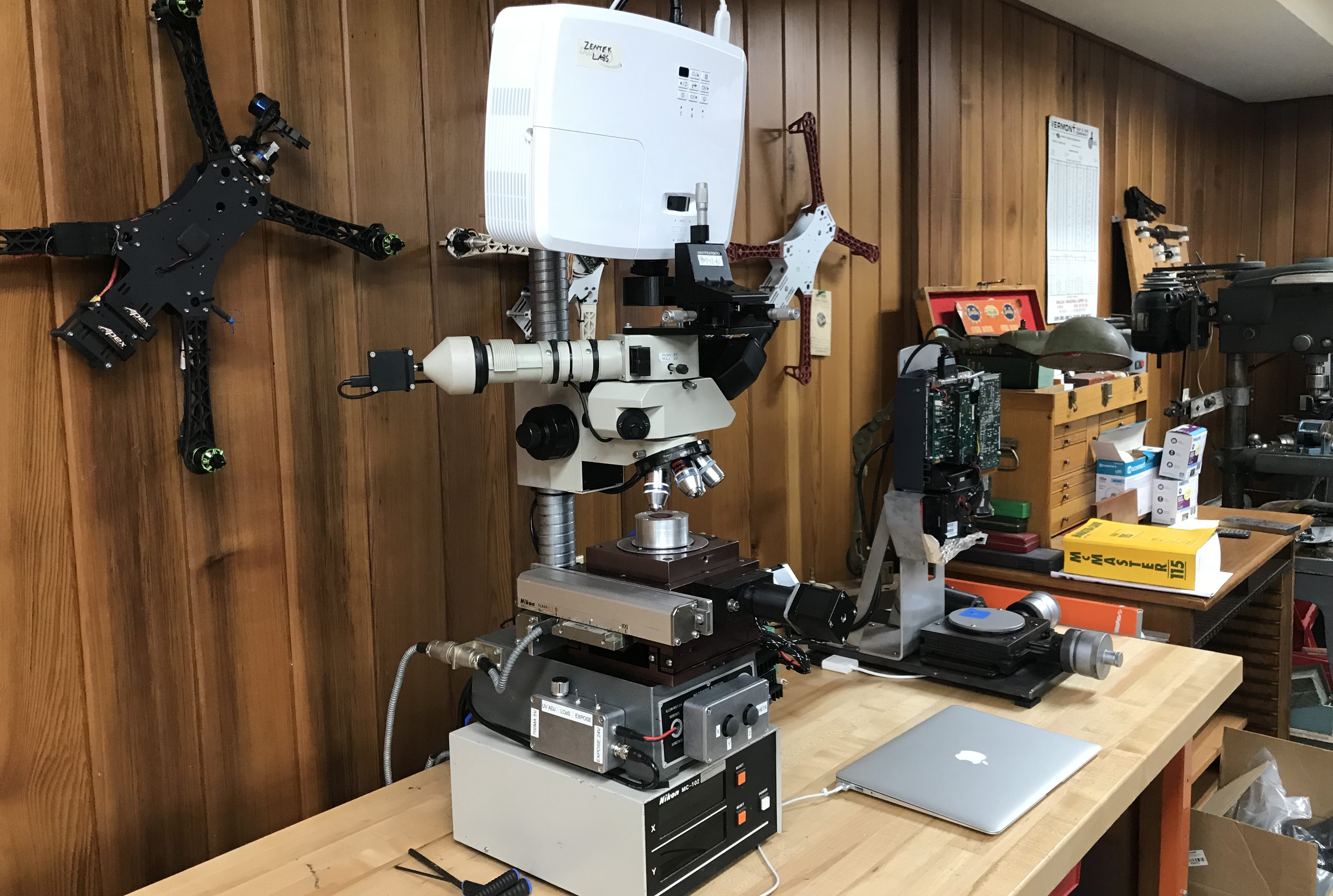


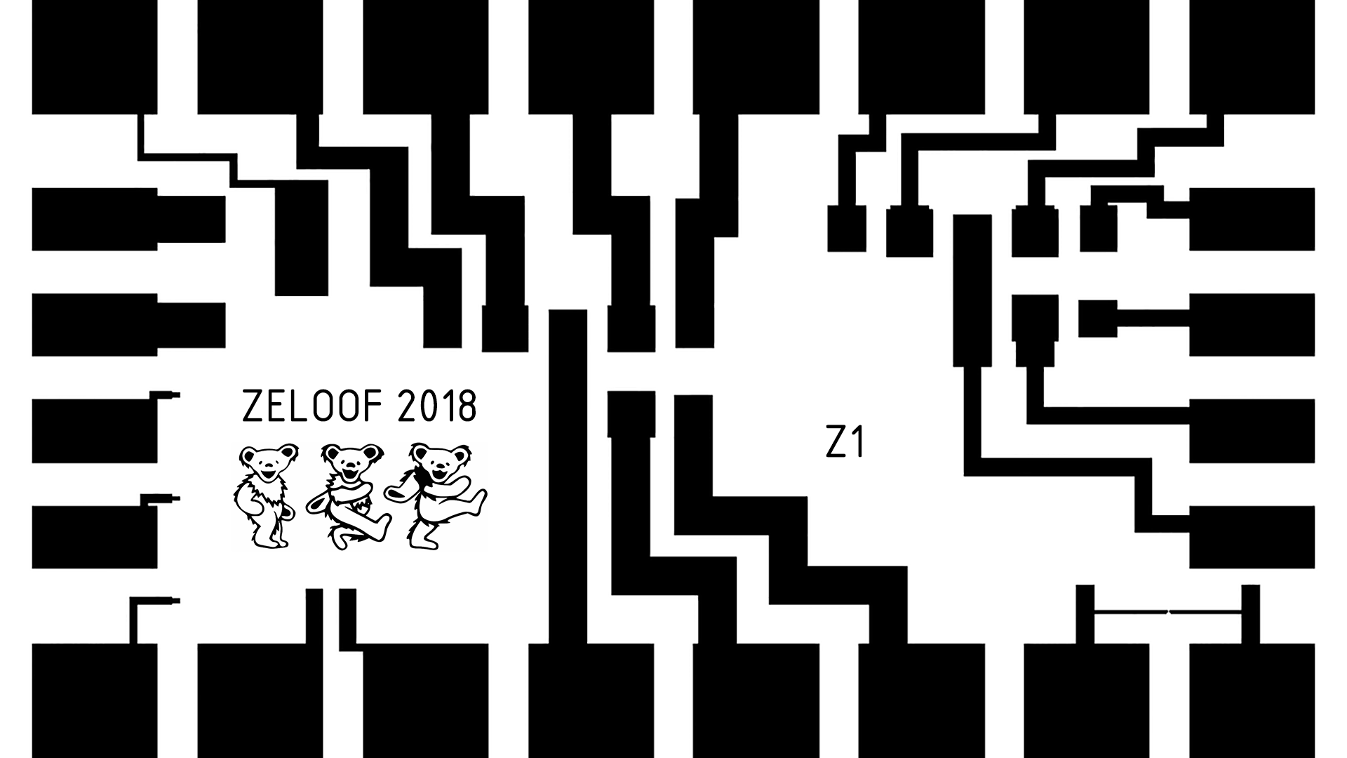
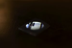
The second and third images above are composed of 4 precisely aligned exposures which enables submicron resolution over large areas. This “true” stepper operation uses a closed-loop feedback system and computer visual alignment.

Issues with non-uniform UV intensity across the exposure field were corrected by applying a mask to each projected image, described here. Proper results were achieved through many trials of different parameters:

Mark III:
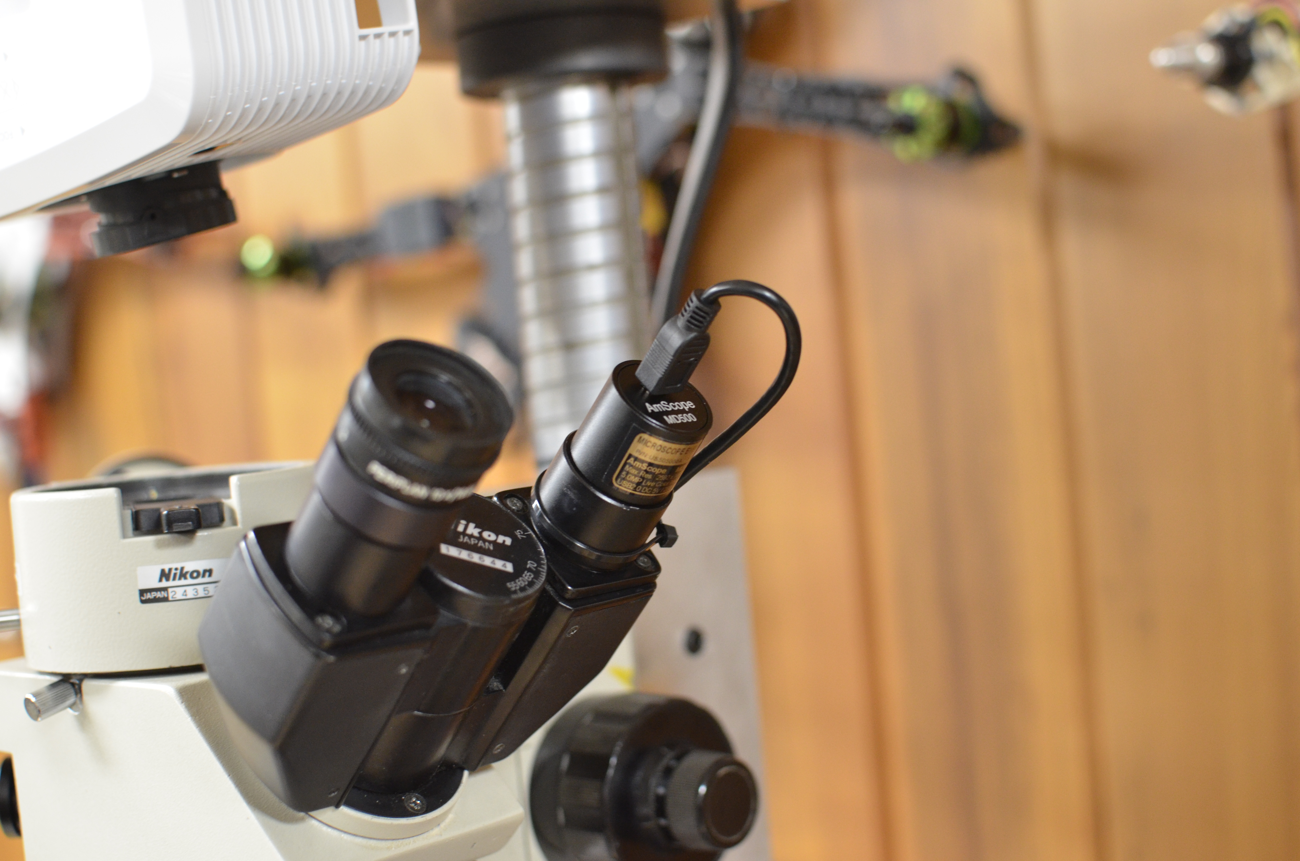
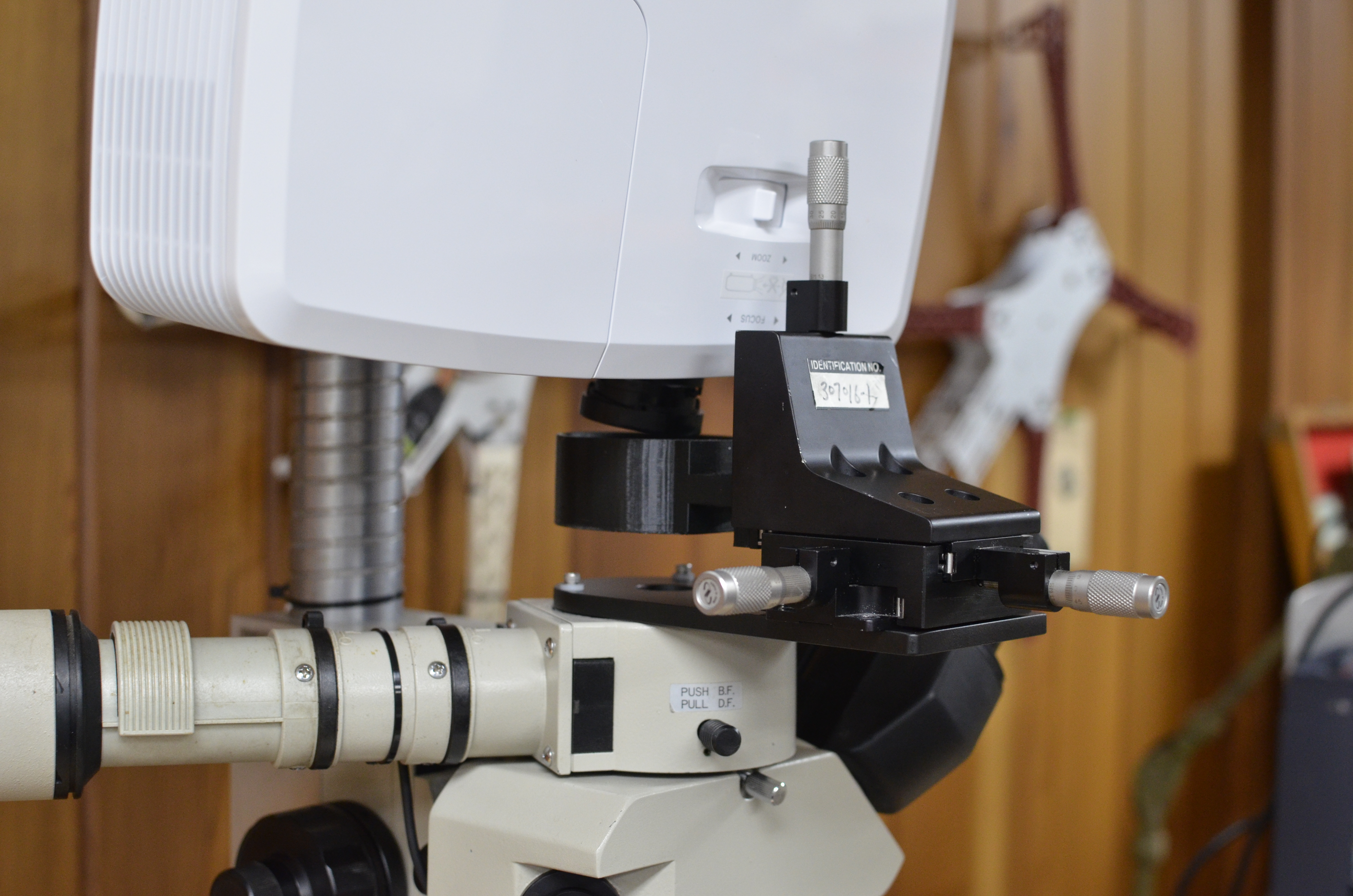
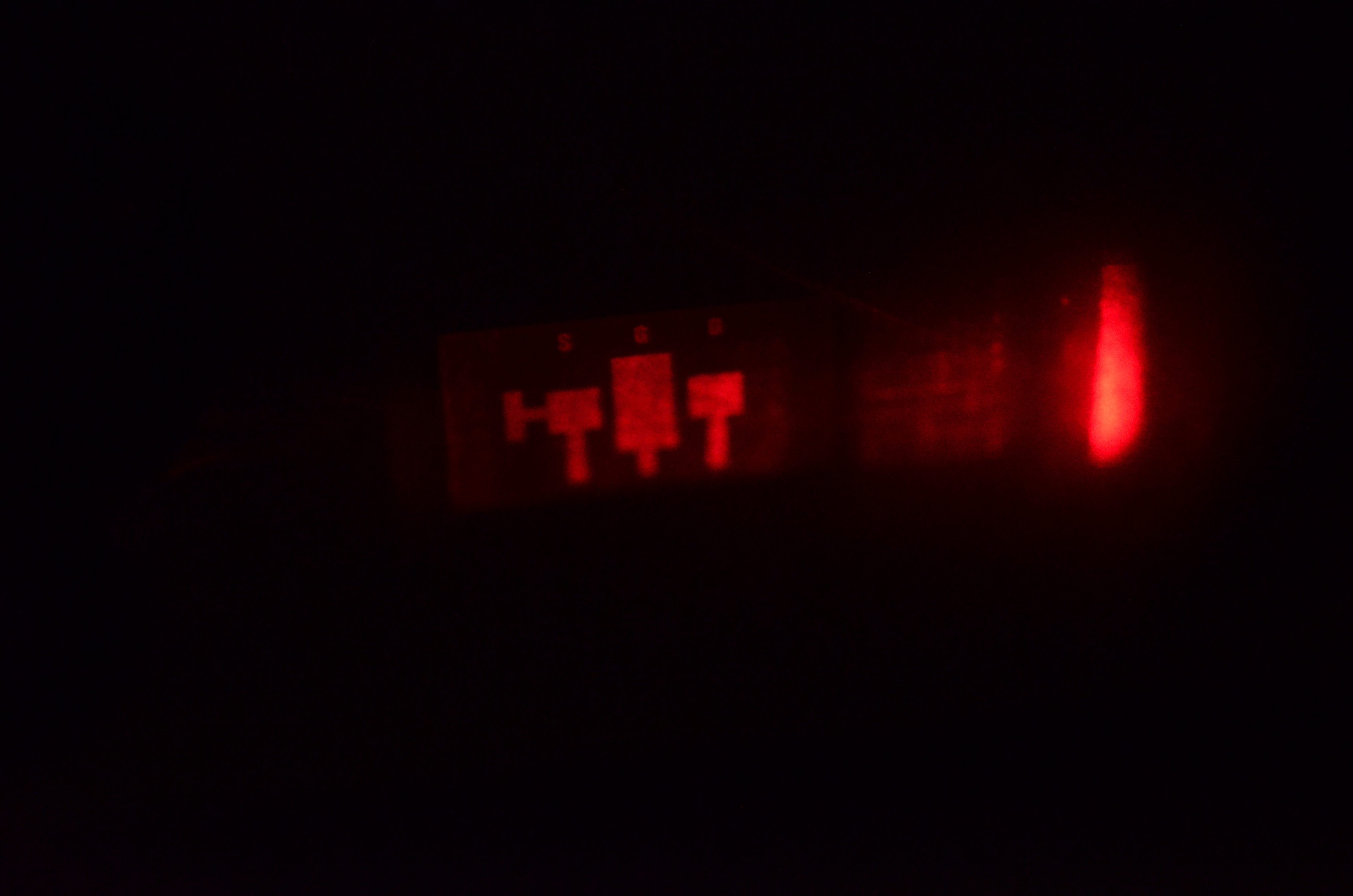
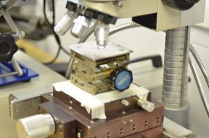
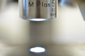
Manual LCoS submicron stepper with red laser alignment illumination. Given a numerical aperture of 0.98 on the microscope objective and with an exposure wavelength of 365nm the simple calculated resolution is 0.227um however the actual resolution is probably around 0.5um due to diffraction limitations inherent in this projection system. The depth of focus @ NA = 0.98 is calculated to be approximately 1.8um but is likely worse.


Mark II:
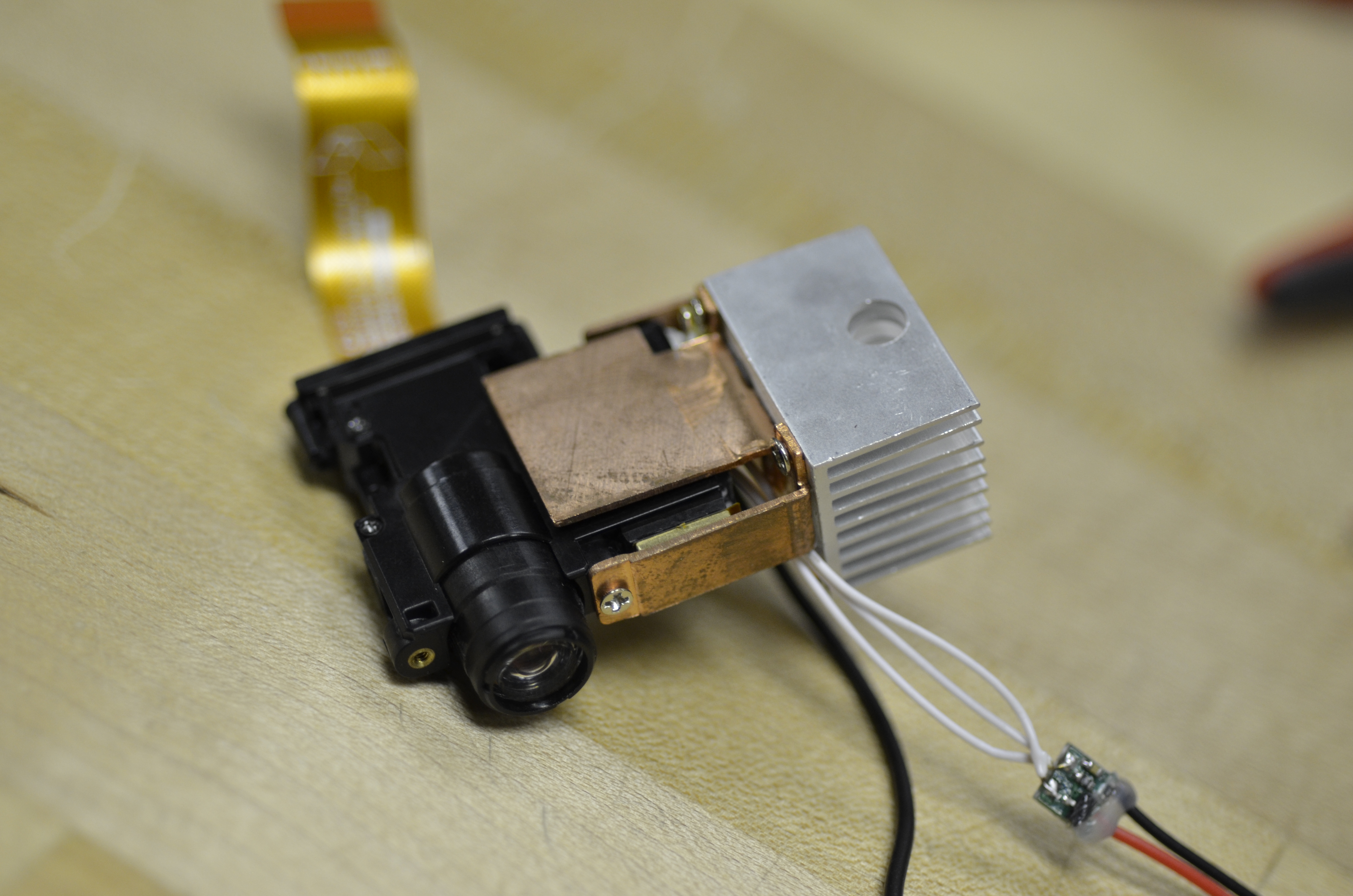
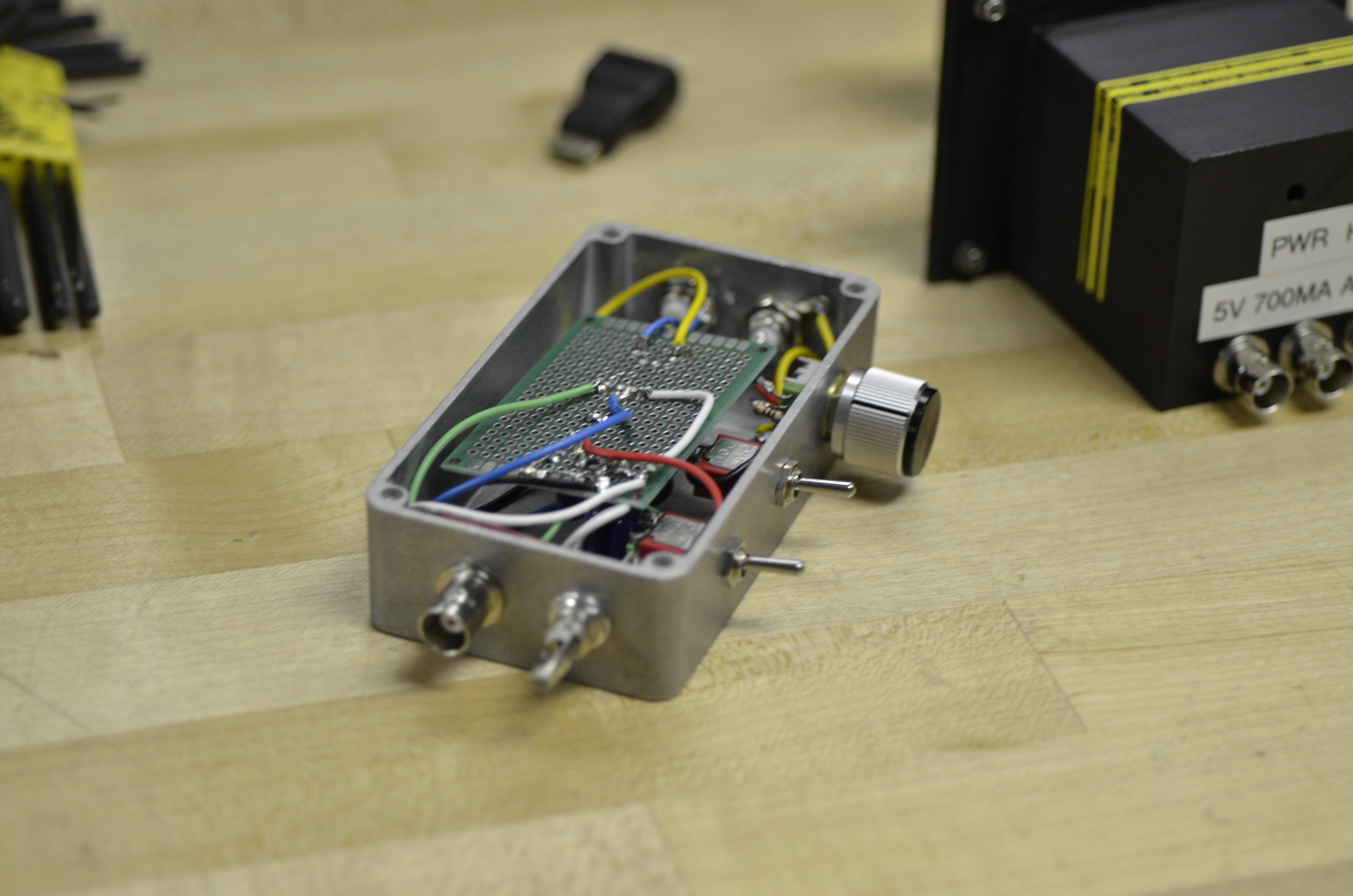
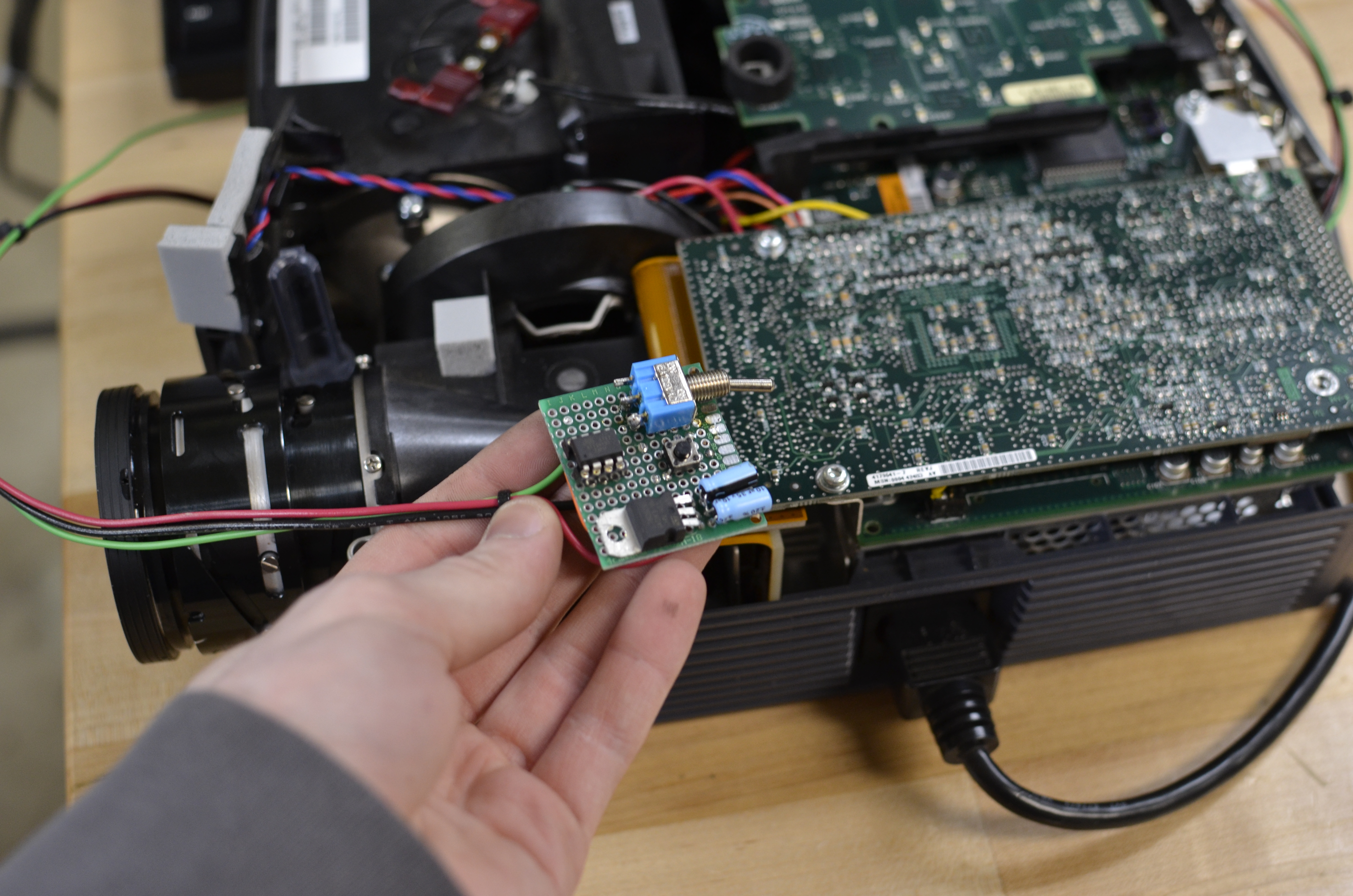
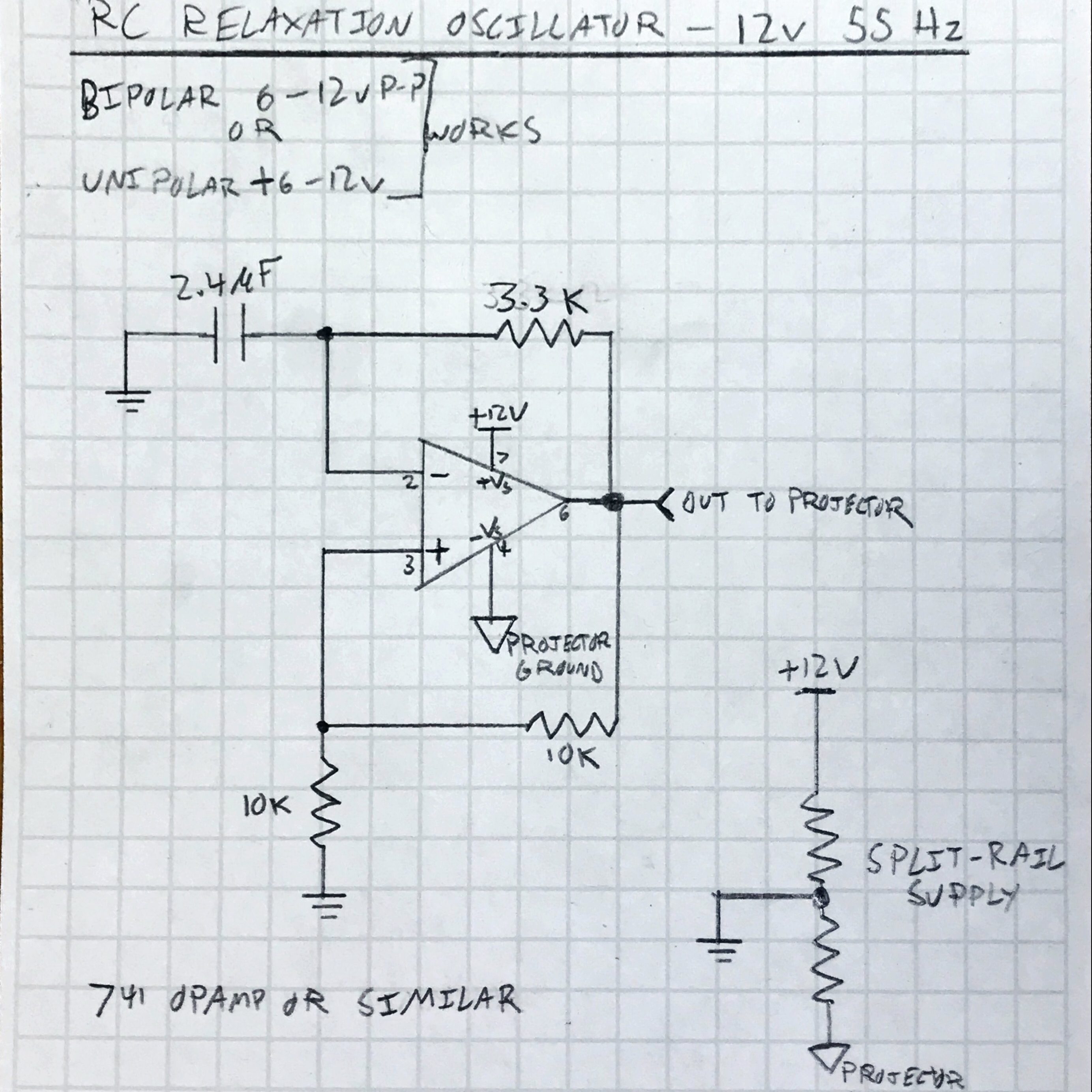
Manual DLP projection aligner >10um features. Color wheel is removed because it did not transmit much light below 400nm. Emulation (relaxation oscillator) circuits were made to reproduce the signals that the projector expected from the color wheel back EMF motor drive/sensor and photodiode.


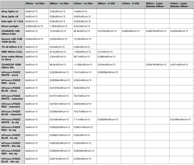
Exposure times calculated by integration of total UV dosage measured at different wavelengths with the radiometer. To calculate exposure time for AZ4210 resist, for example, the datasheet is consulted to see a recommended dose of around 135 mJ/cm^2 for a 3.5um film thickness. If exposed with a 5x objective on my system, the exposure time @ 410nm is (135 mJ/cm^2)/(4.05mW/cm^2) = approx. 33 seconds. This is a bit longer than I would like but given that it is a positive resist that is to be expected.

Mark I:
Proof-of-concept DLP setup

Holycrap dude.
what the heck
Hi Sam I have see your work on homemade transistors and IC’s. As well as Jeri Ellsworth’s work. I have a question about maskless lithography. I have a Laborlux D trinocular microscope and DLP projector. I was wondering about your reduction optics it appears to be on the Mark II a 3d printed adapter housing, it looks like a macro lens and adapter inside of that. Do you have any information about the lens your using and whether the lens sizes adhere to some size standard. I also like your new setup with the Pico DLP. Any information you can share will be greatly appreciated it would also be nice to build a friendship with someone who has similar interests. My initial goal is to see if maskless with work on PCB’s or other materials then once I have other equipment I will try working with semiconductors. So basically i’m looking for information about your exact lens rig for this Mark II design thanks.
Wow, the capabilities of your lab match some of the semicon research institutes out there.
What does it take to get something like this set up?
PCB-s could be exposed as well, without the microscope?
Have you thought about switching from microscope to projection lens for higher resolution? 1:1.6 X10 reduction comes up at eBay from time to time for around 500$.