Details and photos of my newest maskless photolithography stepper have been posted here: Info Page
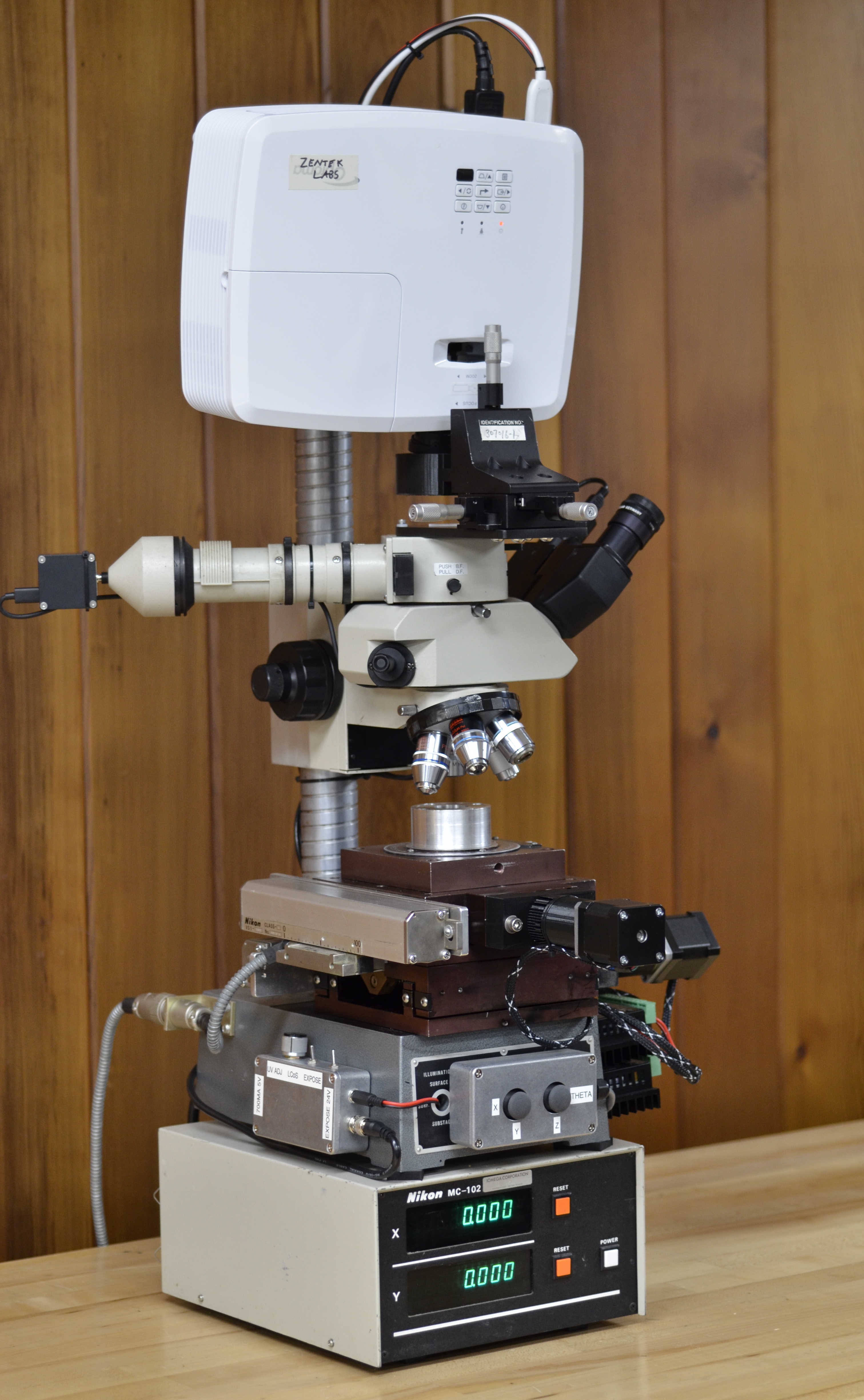
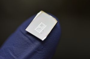
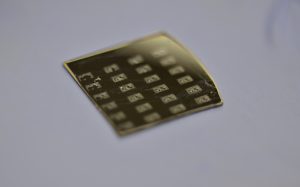
Automated DLP submicron stepper for 2″ (50mm) wafers with LabView control, computer alignment, and wafer vacuum chuck. Based on an old Nikon microscope with custom optics and in-situ UV-VIS spectroscopy for illumination process control. Diffraction-limited resolution is <250nm with a 365nm light source.

Phish dancing bears! This is amazing!
你们非常厉害!
我们组现也准备做无掩膜工艺的研究。
现在卡在无掩膜如何实现(LCD用紫外的话会被紫外改性,能用的DLP设备(能透过紫外)不是一个中国的中学生(我)能负担的起的)和载片台的定位精度(套刻对准),以及到亚微米(.18、.25um)(有可能会深入到纳米(nm))时的晶片观察(电镜?在中国这不是个人容易买到的东西(应该说至少不是一般中学生买得起的(实在是太贵了)))。
(以上提到的均为半导体组亚微米工设备组现在面临的问题)
我希望我们能讨论(邮箱你应该看得到吧)
【I hope we can discuss it together(I think you should see the email of me)】
Hi, I’m happy to help, please email me at sam@zeloof.xyz so we can discuss
Its really incredible!
I am also fond of some silicon gadgets, while I am not really understand how to make sure the position of the wafer is precise enough during photolithography, and I also have some problems with maskless photolithography technique.