I started a company – And we’re hiring
Contribute to the open source project – HackerFab. Join the Discord
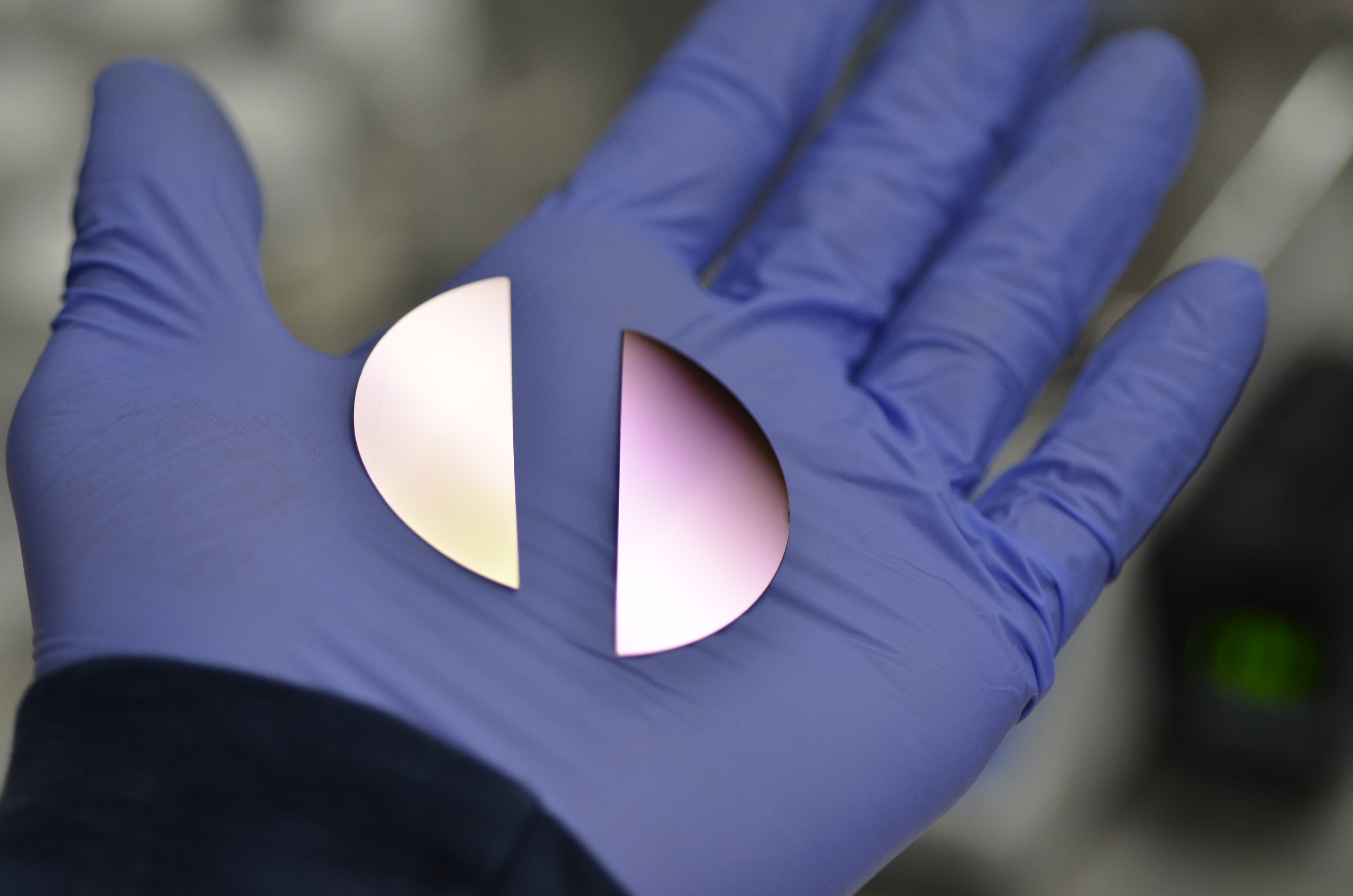
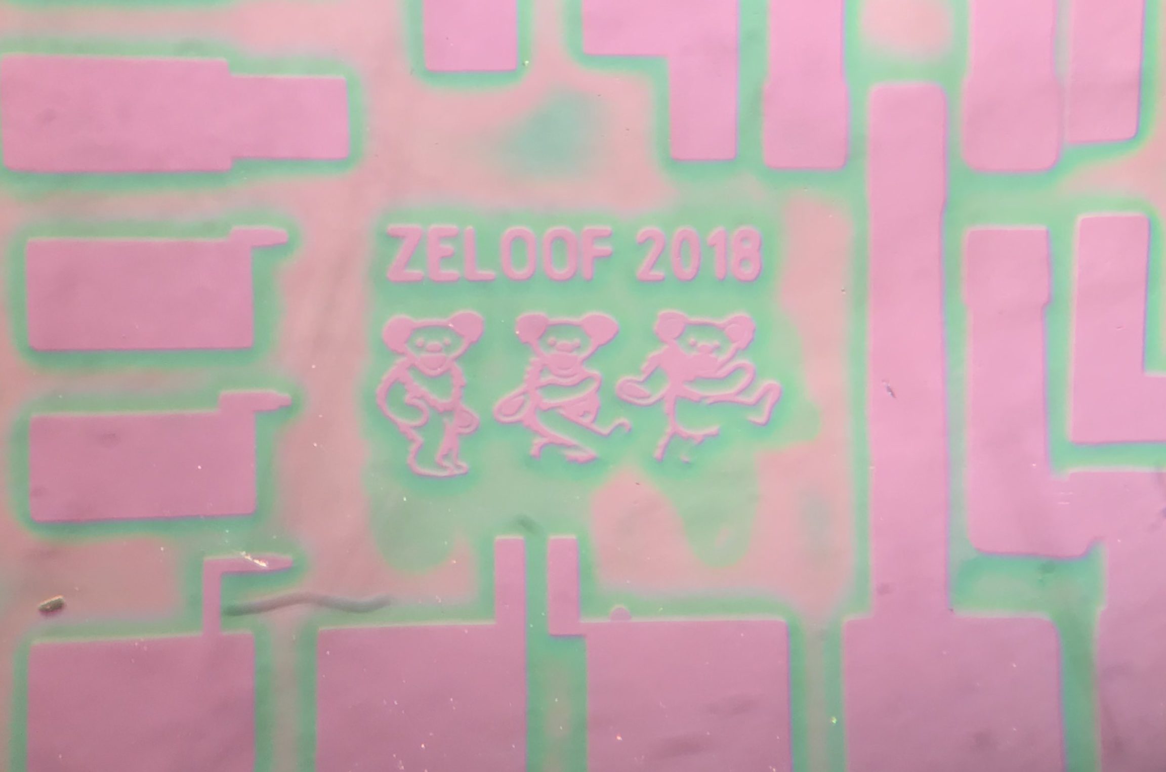
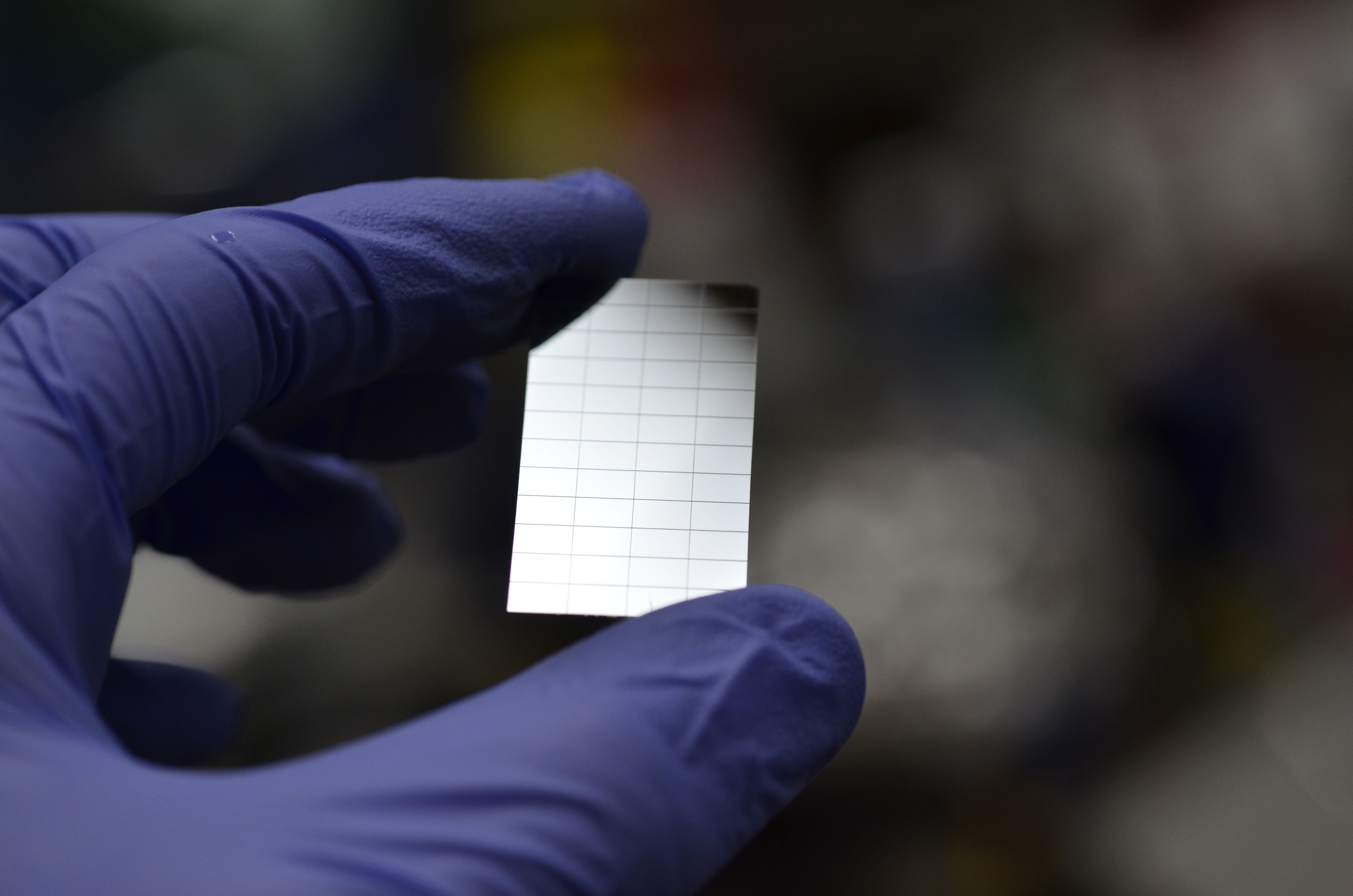
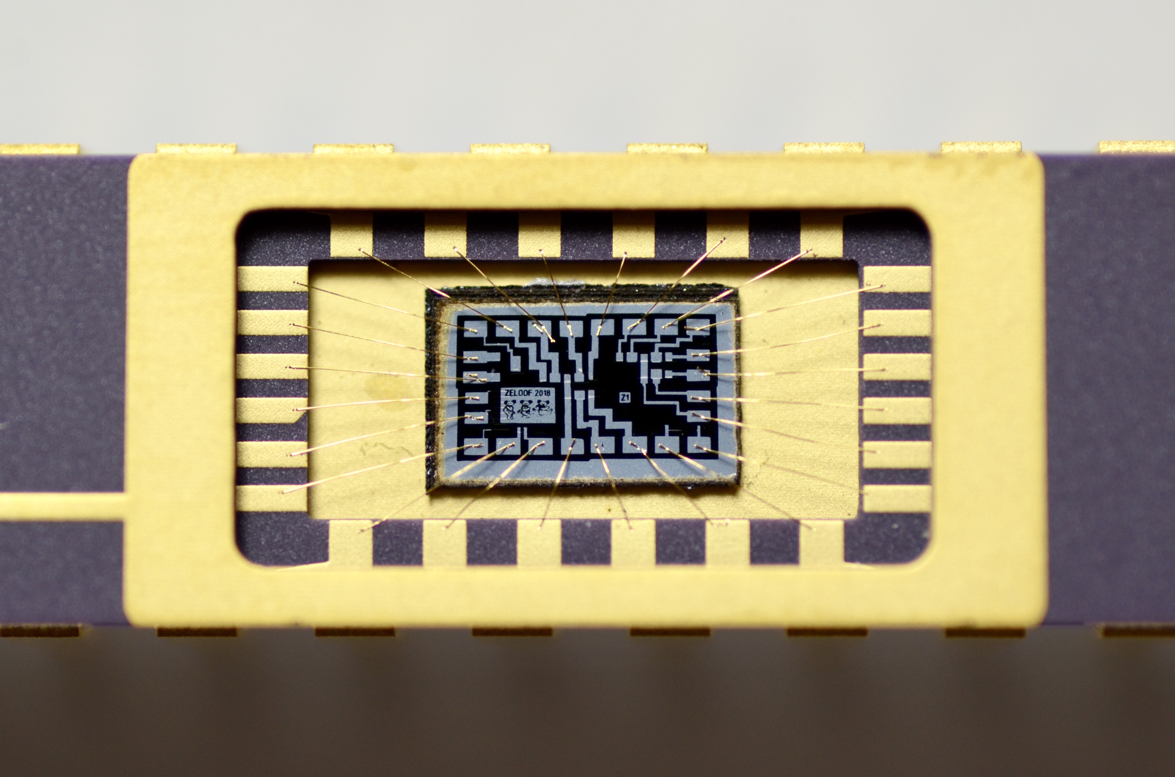
Homemade 1000+ transistor array chip
In 2018 I made the first lithographically fabricated integrated circuits in my garage fab. I was a senior in high school when I made the Z1 amplifier, and now I’m a senior in college so there are some long overdue improvements to the amateur silicon process.
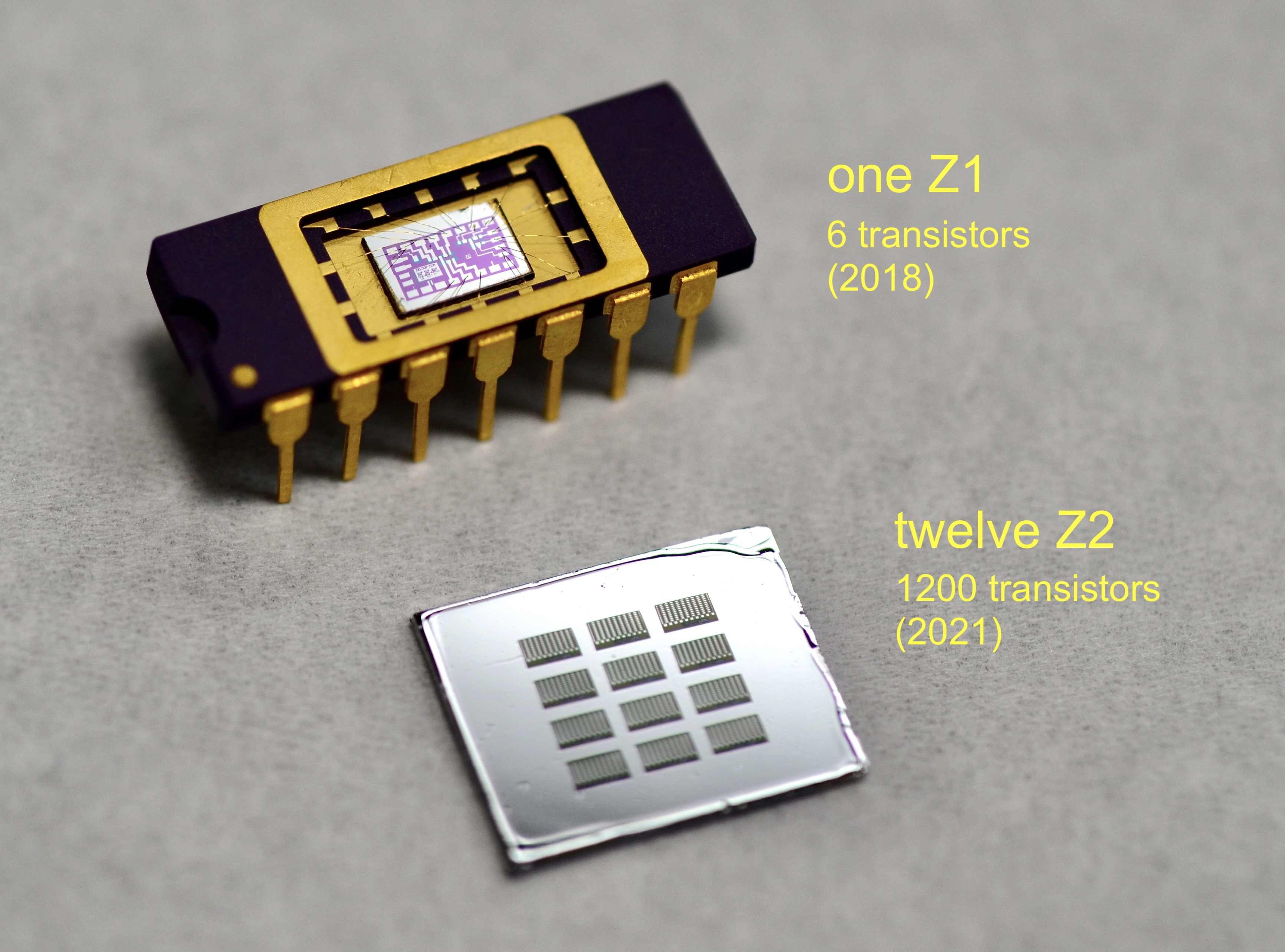
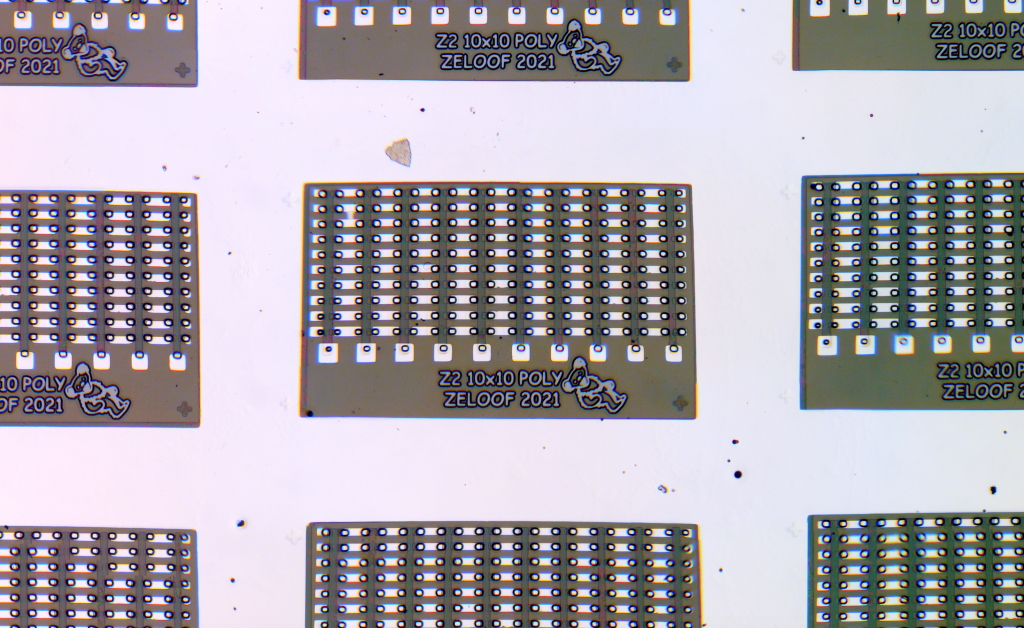
The Z1 had 6 transistors and was a great test chip to develop all the processes and equipment. The Z2 has 100 transistors on a 10µm polysilicon gate process – same technology as Intel’s first processor. My chip is a simple 10×10 array of transistors to test, characterize, and tweak the process but this is a huge step closer to more advanced DIY computer chips. The Intel 4004 has 2,200 transistors and I’ve now made 1,200 on the same piece of silicon.

Previously, I made chips with a metal gate process. The aluminum gate has a large work function difference with the silicon channel beneath it which results in a high threshold voltage (>10V). I used these metal gate transistors in a few fun projects like a guitar distortion pedal and a ring oscillator LED blinker but both of these required one or two 9V batteries to run the circuit due to high Vth. By switching to a polysilicon gate process, I get a ton of performance benefits (self aligned gate means lower overlap capacitances) including a much lower Vth which makes these chips compatible with 2.5V and 3.3V logic levels. The new FETs have excellent characteristics:
NMOS Electrical Properties:
Vth             = 1.1 V
Vgs MAX         = 8 V
Cgs             = <0.9 pF
Rise/fall time  = <10 ns
On/off ratio    = 4.3e6
Leakage current = 932 pA (Vds=2.5V)
I was particularly surprised by the super low leakage current. This value goes up about 100x in ambient room lighting.


Now we know that it’s possible to make really good transistors with impure chemicals, no cleanroom, and homemade equipment. Of course, yield and process repeatability are diminished. I’ll do more testing to collect data on the statistics and variability of FET properties but it’s looking good!

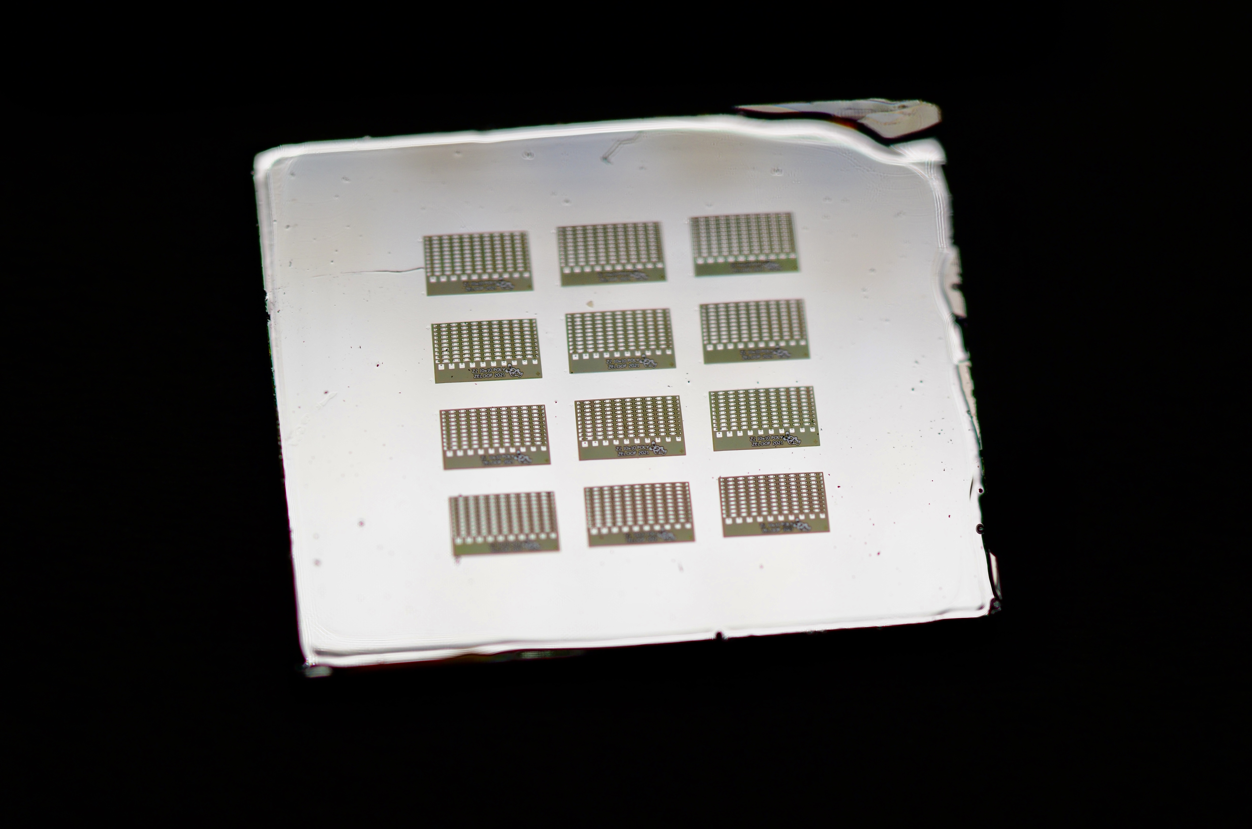
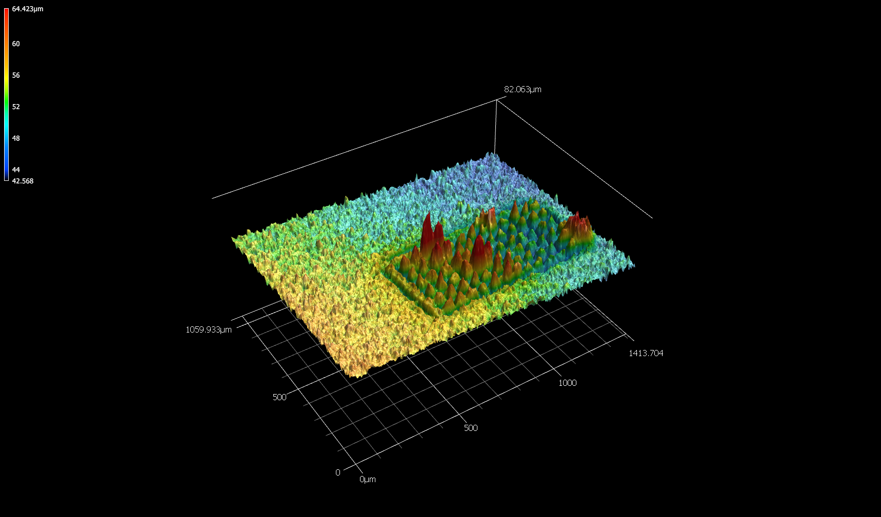
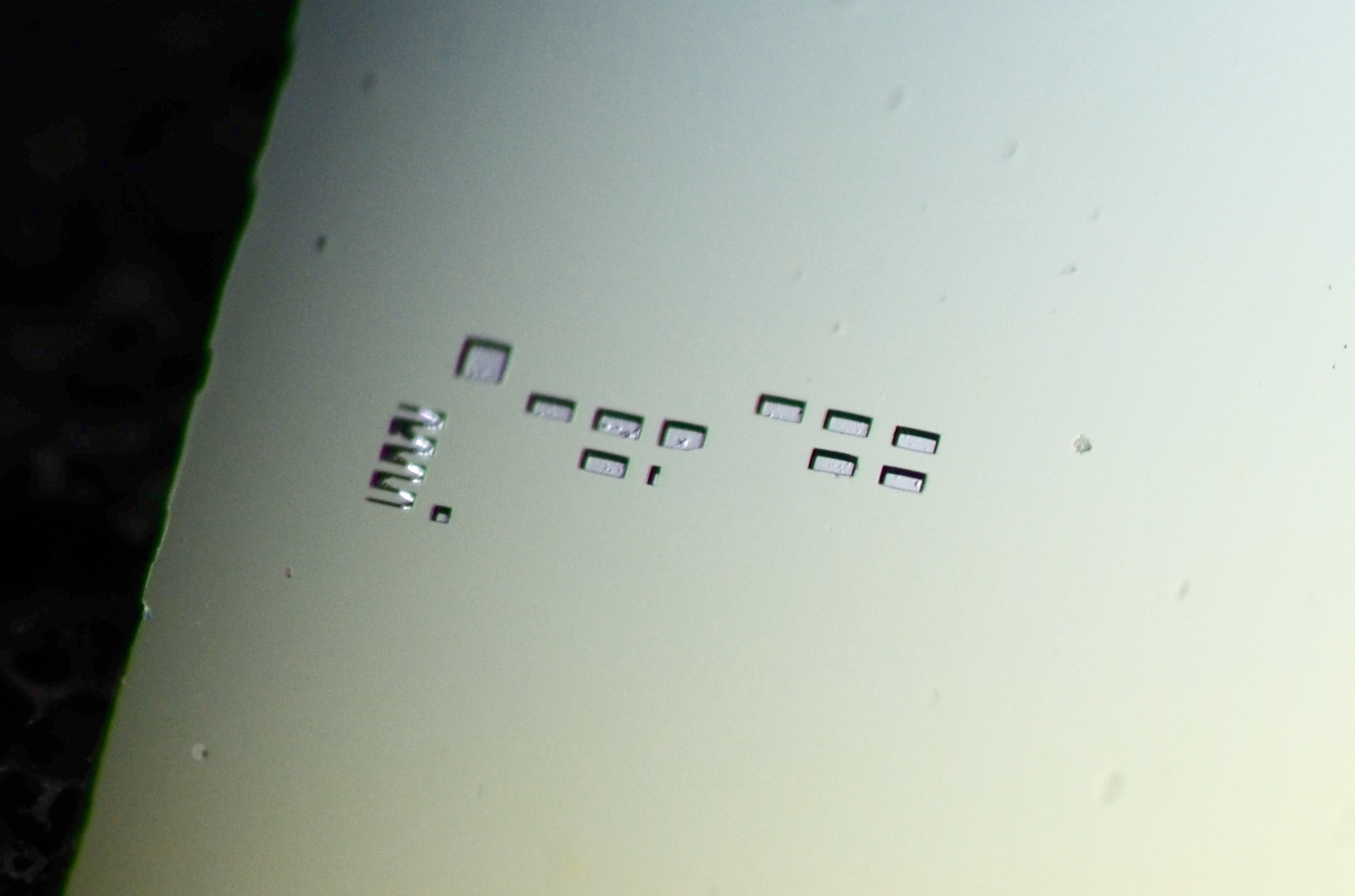
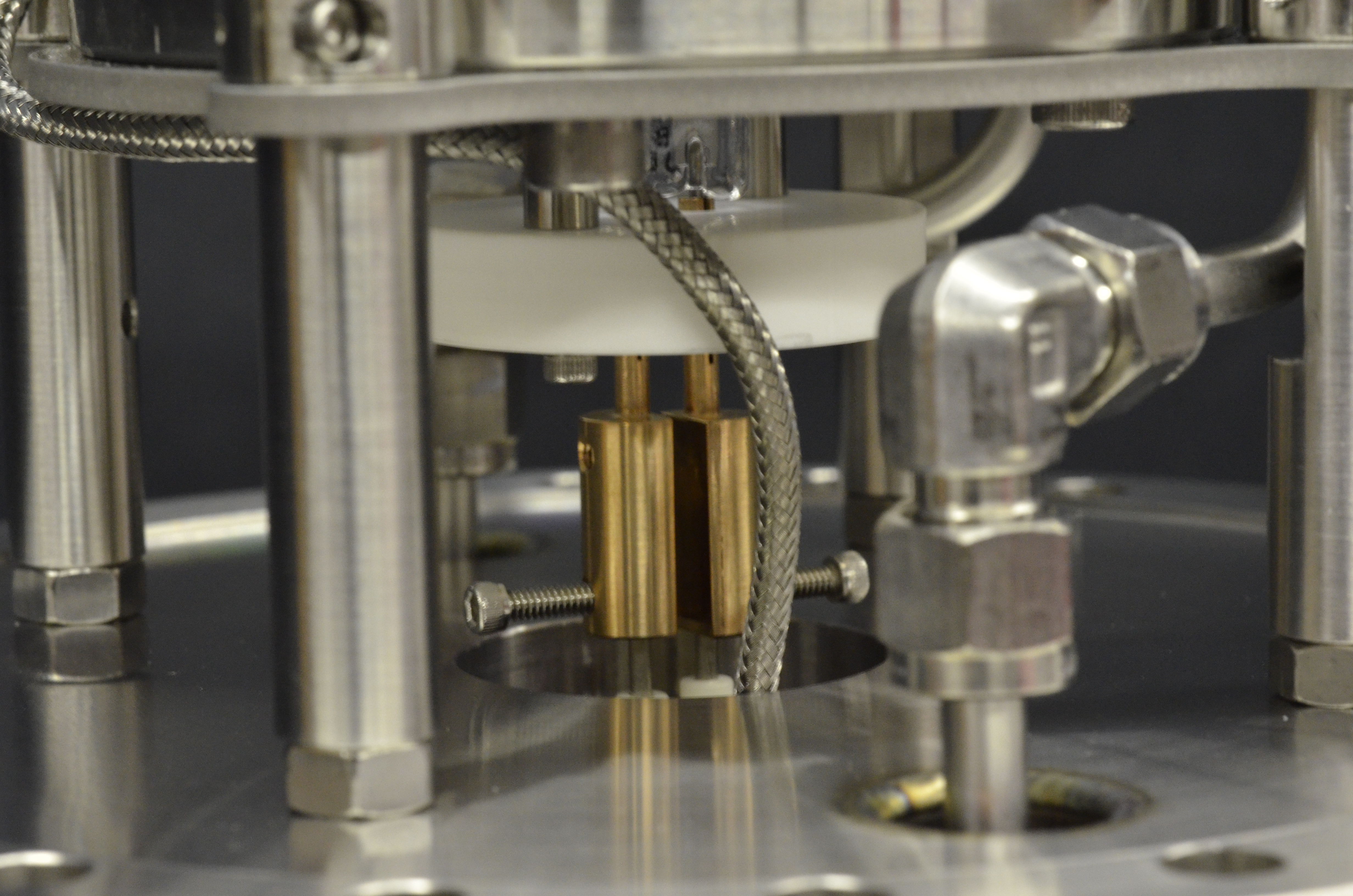
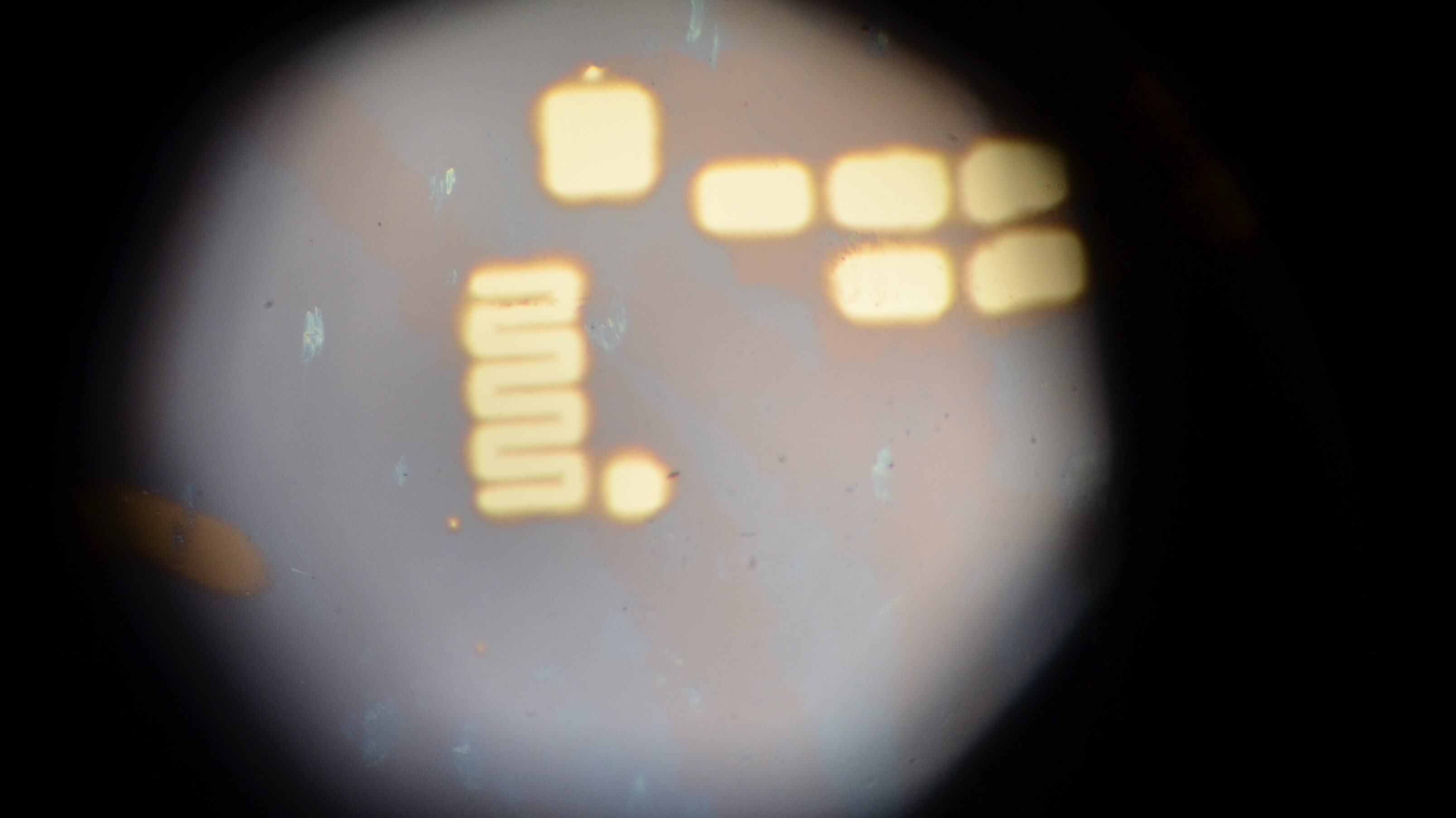
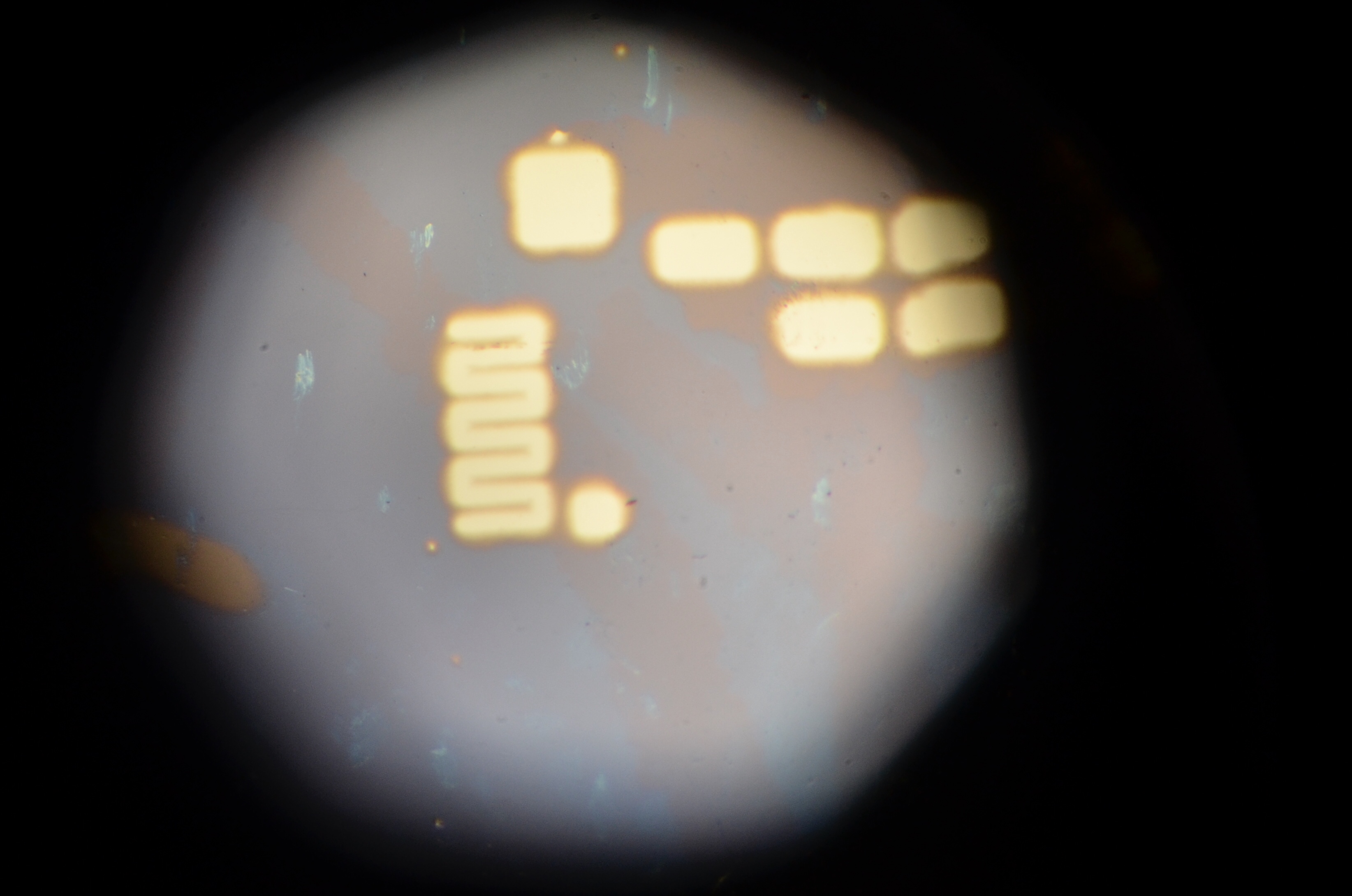
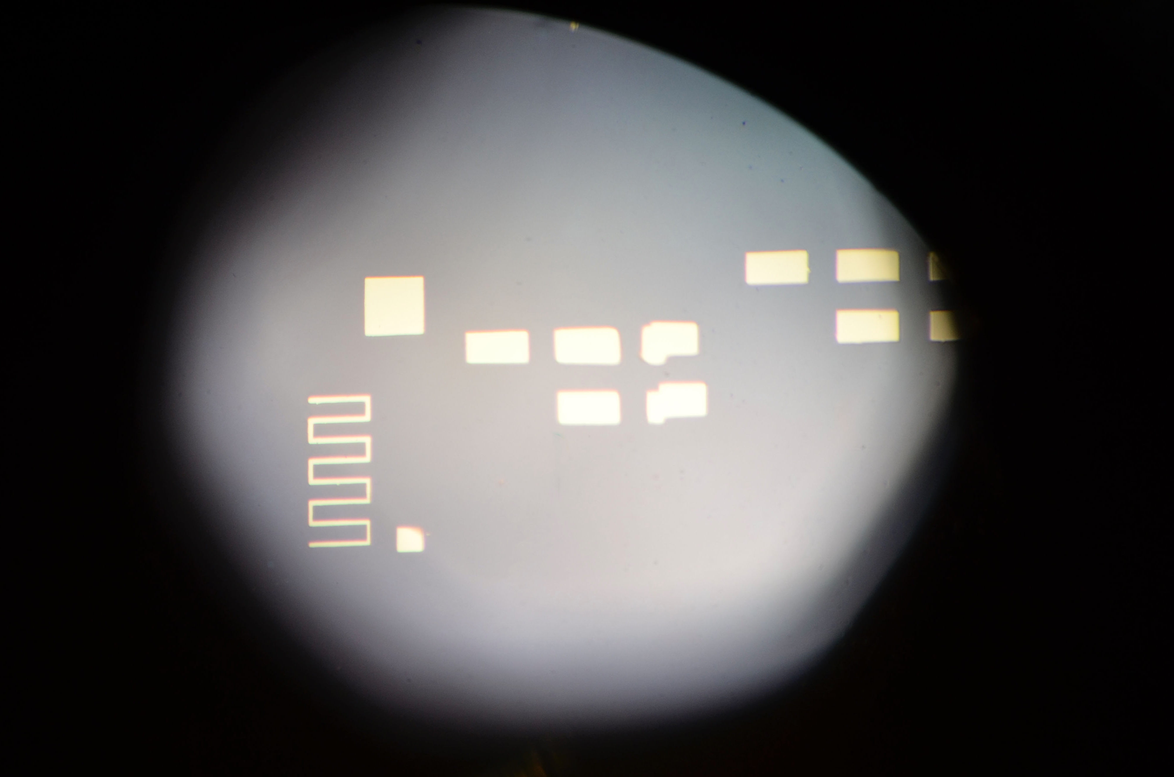
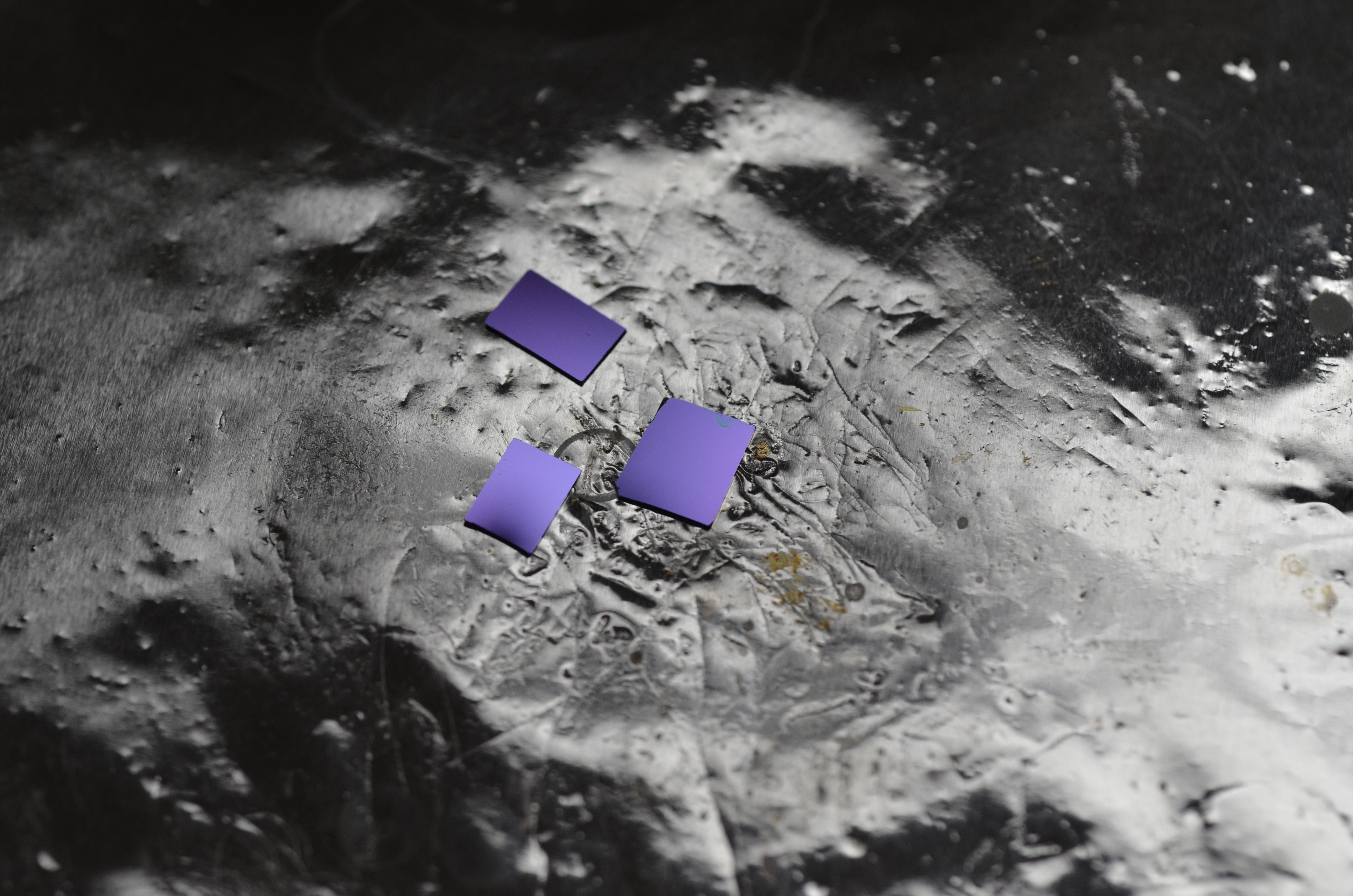
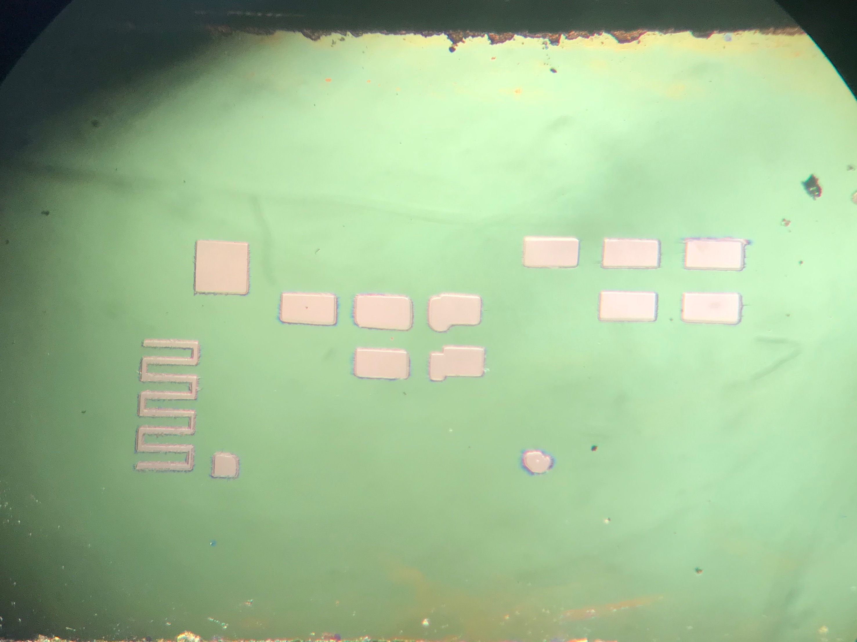
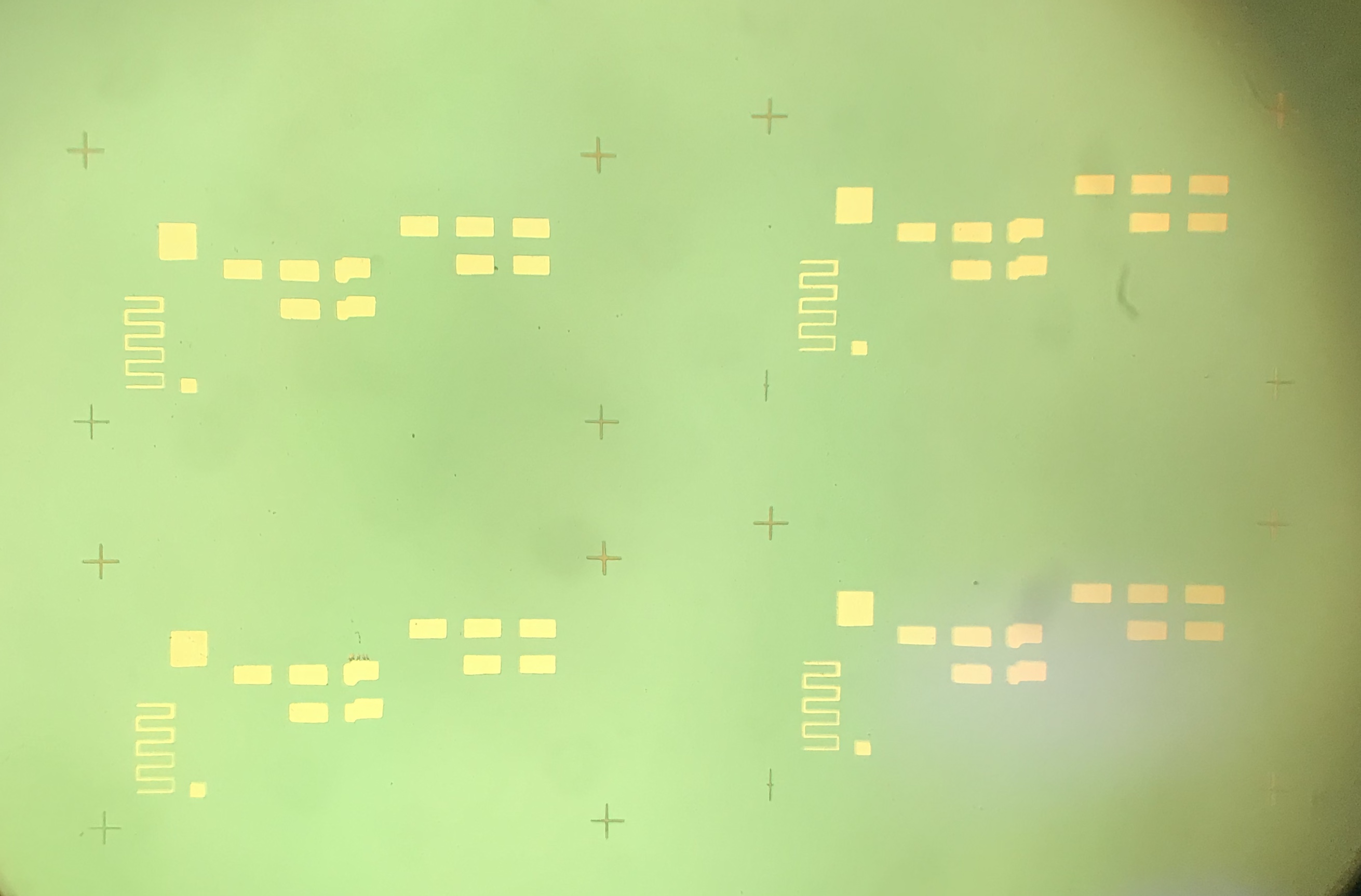
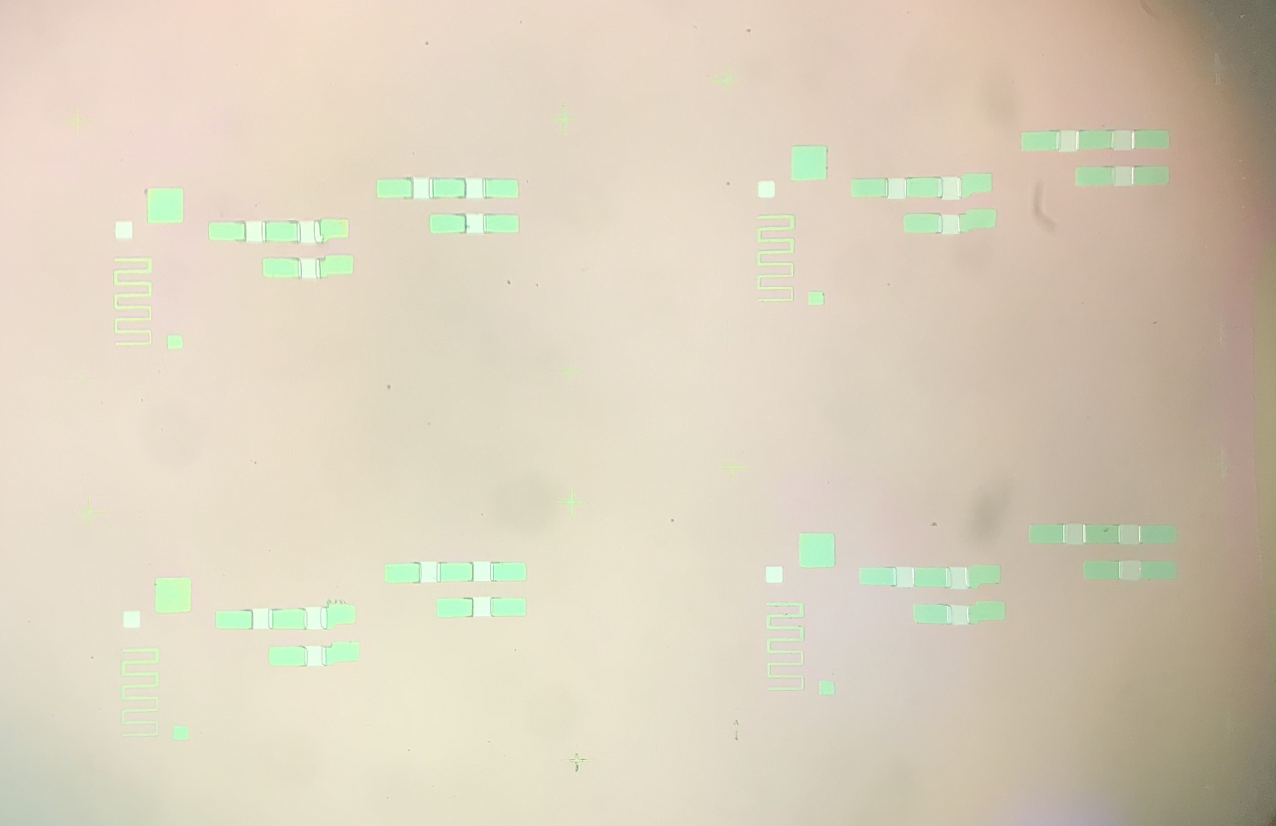
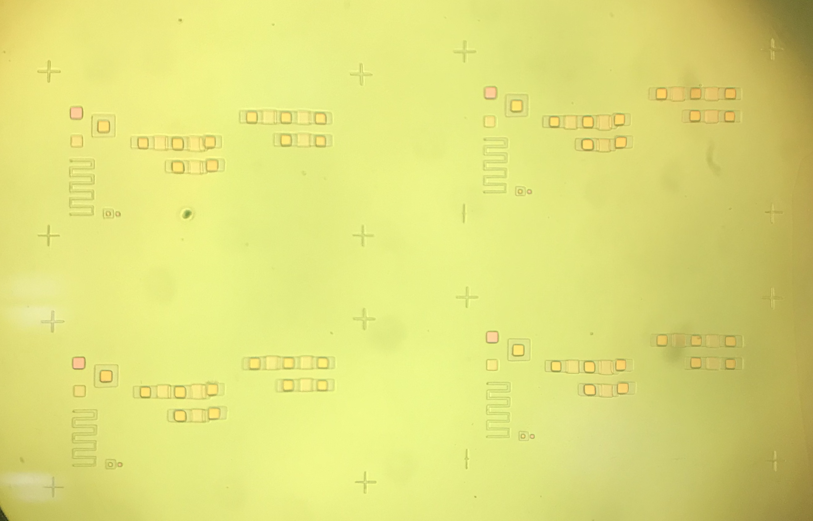
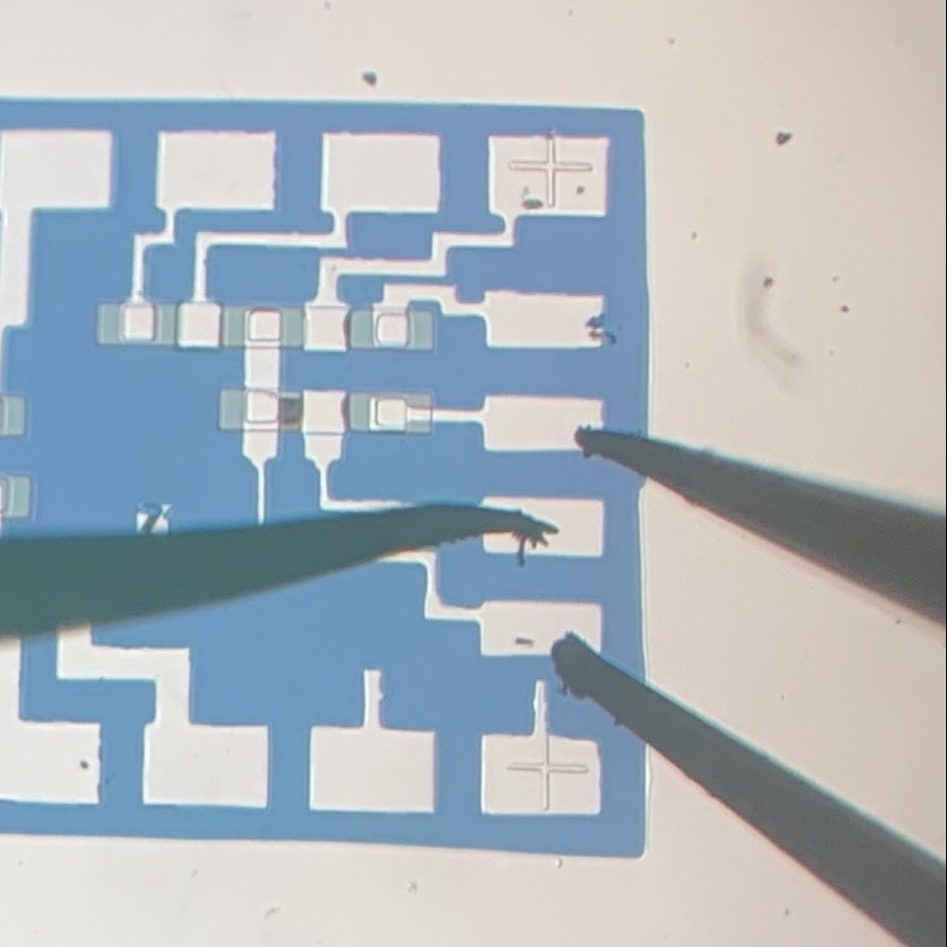
The chip is small, about one quarter the die area of my previous ICs (2.4mm^2) which makes it hard to probe. There’s a simple 10×10 array of N-channel FETs on each chip which will give me a lot of characterization data. Since it’s such a simple design, I was able to lay it out using Photoshop. Columns of 10 transistors share a common gate connection and each row is strung together in series with adjacent transistors sharing a source/drain terminal. It’s similar to NAND flash but I only did this to keep the metal pads large enough so I can reasonably probe them, if every FET had 3 pads for itself they would be too small.
It’s hard to convey the excitement of seeing a good FET curve displayed on the curve tracer after dipping a shard of rock into chemicals all day.


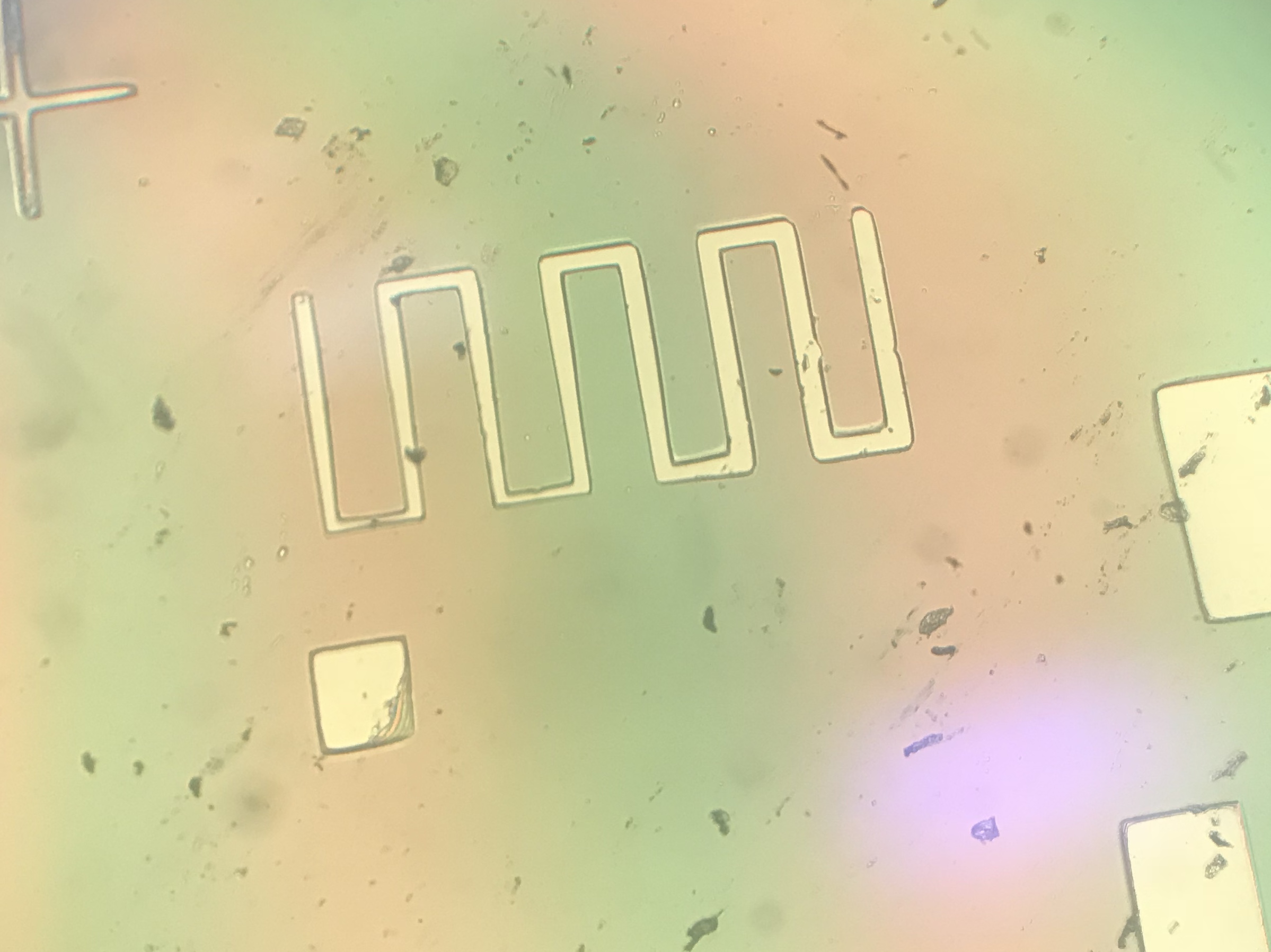
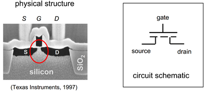
A single 10µm NMOS transistor can be see below, with slight misalignment in the metal layer (part of the left contact is uncovered). Red outline is polycrystalline silicon, blue is the source/drain.


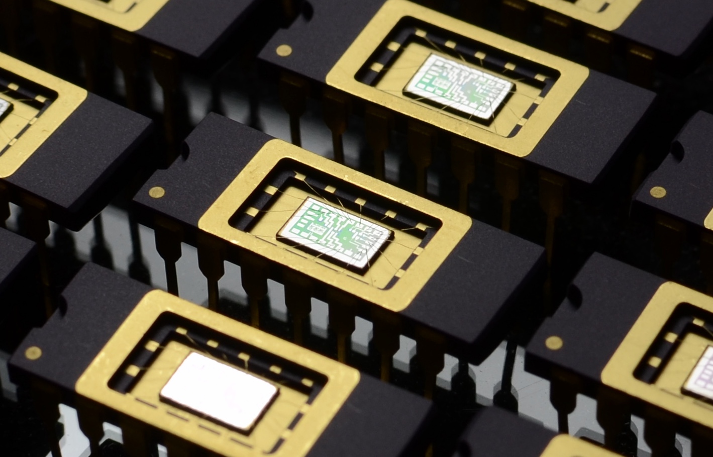
So far I’ve made an opamp (Z1) and a memory-like array (Z2). More interesting circuits are definitely possible even with this low transistor density. The process needs some tweaking but now that I’m able to consistently make good quality transistors I should be able to design more complex digital and analog circuits. Testing each chip is very tedious so I am trying to automate the process and I’ll post more data then. I’ve made 15 chips (1,500 transistors) and know there’s at least one completely functional chip and at least two “mostly functional”, meaning ~80% of the transistors work instead of 100%. No proper yield data yet. The most common defect is a drain or source shorted to the bulk silicon channel, not a leaky or shorted gate like on my Z1 process.

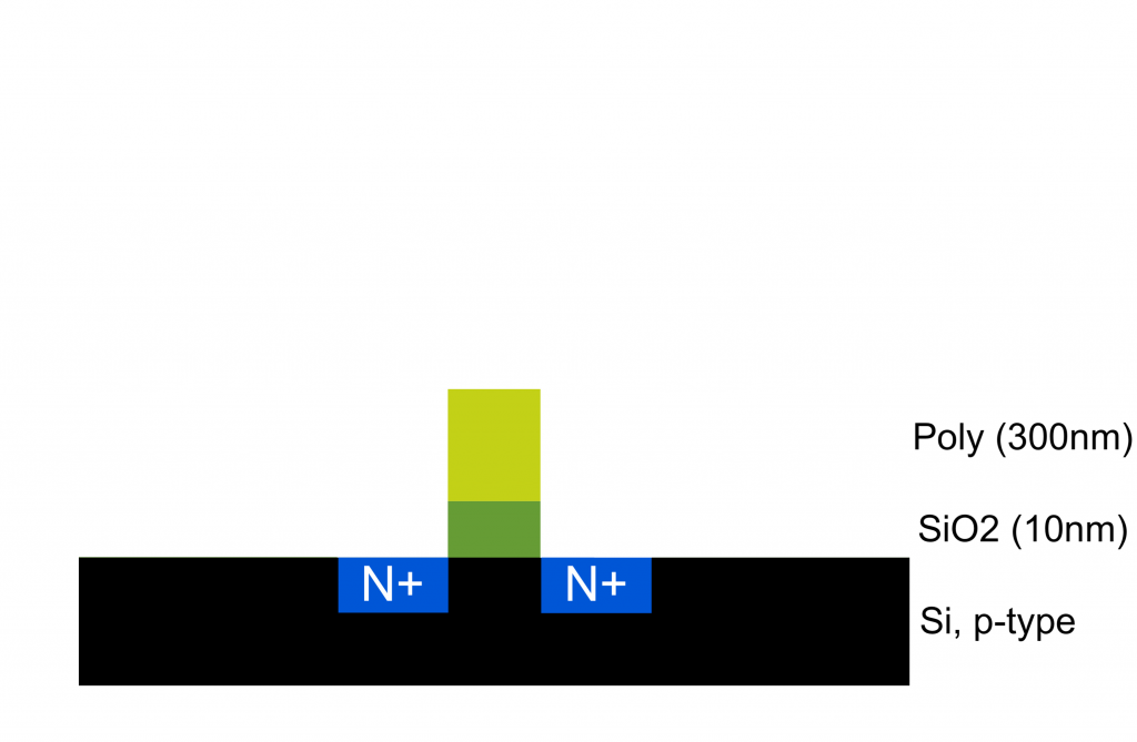
I said before that the gate used to be made out of aluminum and now it’s silicon which makes the chips work a lot better. Silicon comes in three varieties that we care about: amorphous, polycrystalline, and monocrystalline. From left to right, these become more electrically conductive but also much harder to deposit. In fact, monocrystalline Si can’t be deposited, you can only grow it in contact with another mono-Si layer as a seed (epitaxy). Since the gate must be deposited on top of an insulating dielectric, poly is the best we can do. We can heavily dope the polysilicon anyway to make it more conductive.


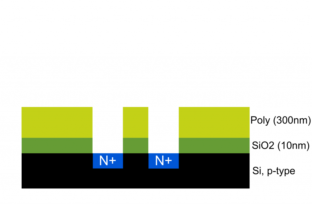
A typical self-aligned polysilicon gate process requires silane, a toxic and explosive gas, to deposit polycrystalline silicon layers. It may also be possible by sputtering or evaporating amorphous silicon and annealing with a laser. A major theme of this DIY silicon process is to circumvent expensive, difficult, or dangerous steps. So, I came up with a modified process flow. It’s a variation on the standard self-aligned methods to allow doping via high temperature diffusion rather than ion implantation. The effect is that I’m able to buy a silicon wafer with the polysilicon already deposited on it from the factory and pattern it to make transistors instead of putting my own polysilicon down halfway through the process. This is a nice short term workaround but it would be best to design a polysilicon deposition process using the laser anneal method mentioned above.
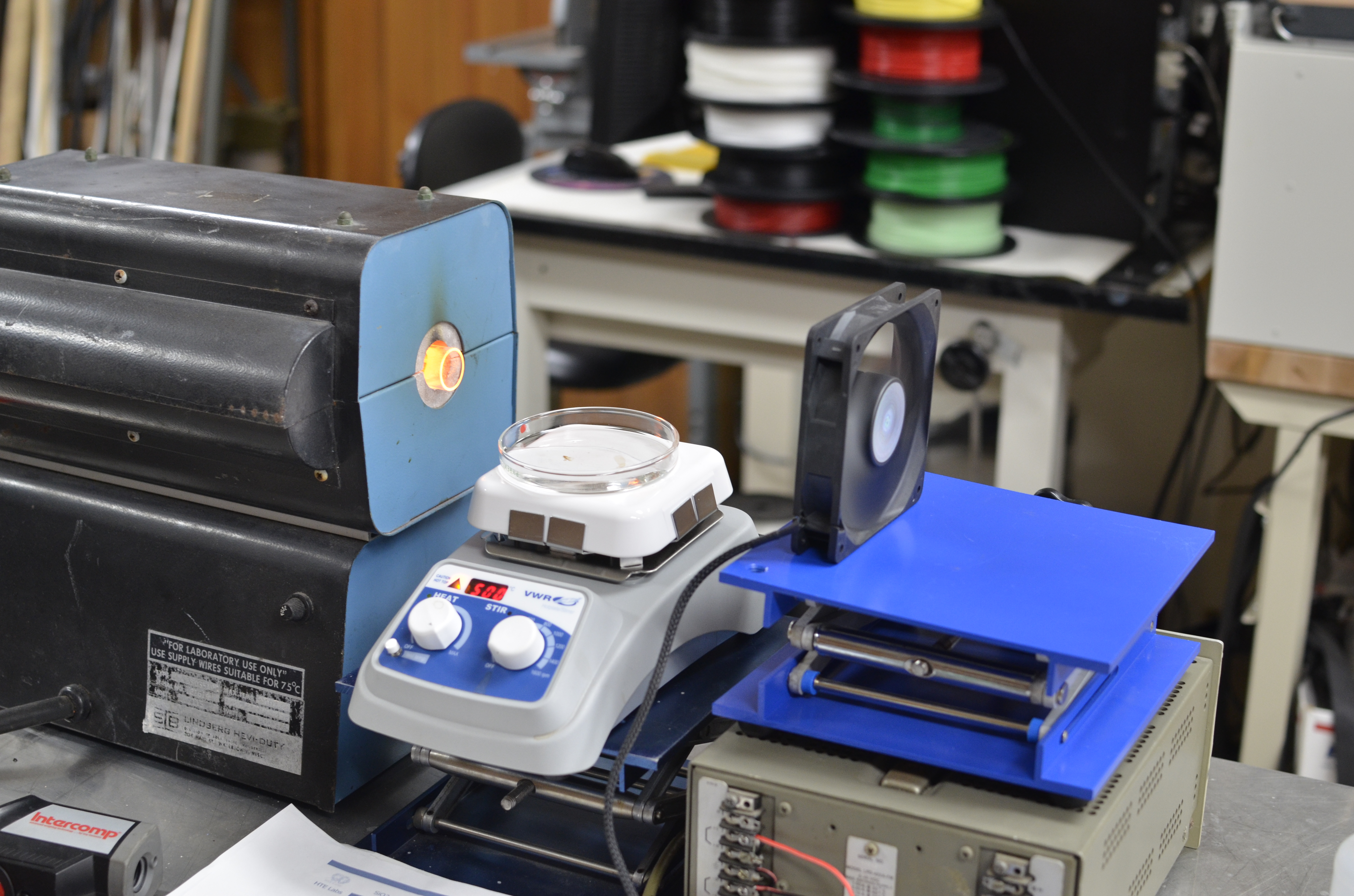
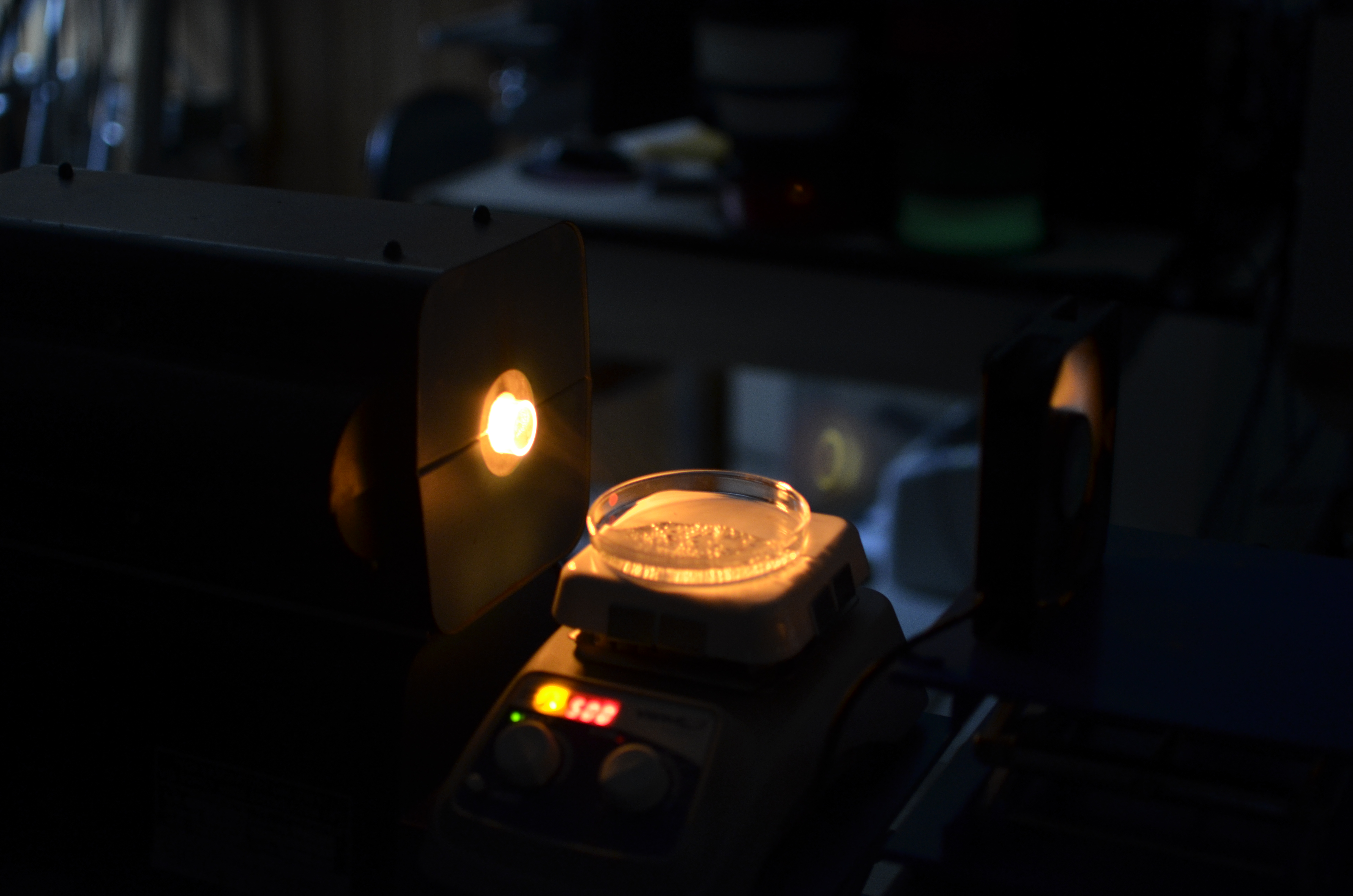
Wafers are available with all kinds of materials deposited on them already, so I just had to find one with a thin layer of SiO2 (gate oxide, ~10nm) followed by a thicker polysilicon (300nm). I found a lot of 25 200mm (EPI, prime, [1-0-0], p-type) wafers on eBay for $45 which is essentially a lifetime supply, so email me if you want one. The gate oxide is the most fragile layer and requires the most care during fabrication. Since I bought the wafer with a nice high quality oxide on it already that was capped off and kept clean by the thick polysilicon layer, I was able to eliminate all the aggressive cleaning chemicals (sulfuric acid, etc) from the process and still make great transistors. Minimal process chemicals and tools are listed below.
Chemicals used in home poly-gate process:
-Water
-Alcohol
-Acetone
-Phosphoric acid
-Photoresist
-Developer (2% KOH)
-N type dopant (filmtronics P509)
-HF (1%) or CF4/CHF3 RIE
-HNO3 for poly etch or SF6 RIE
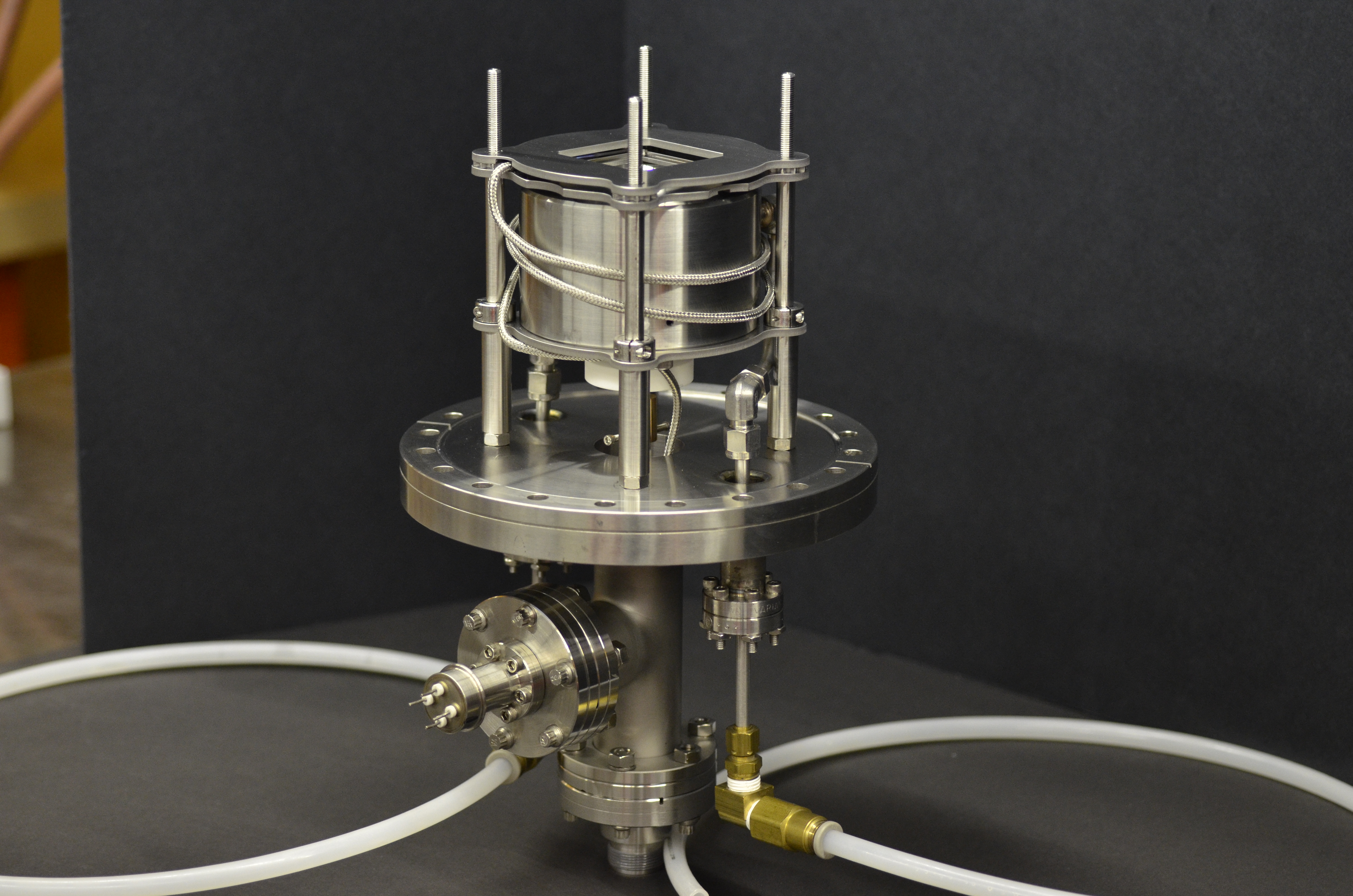
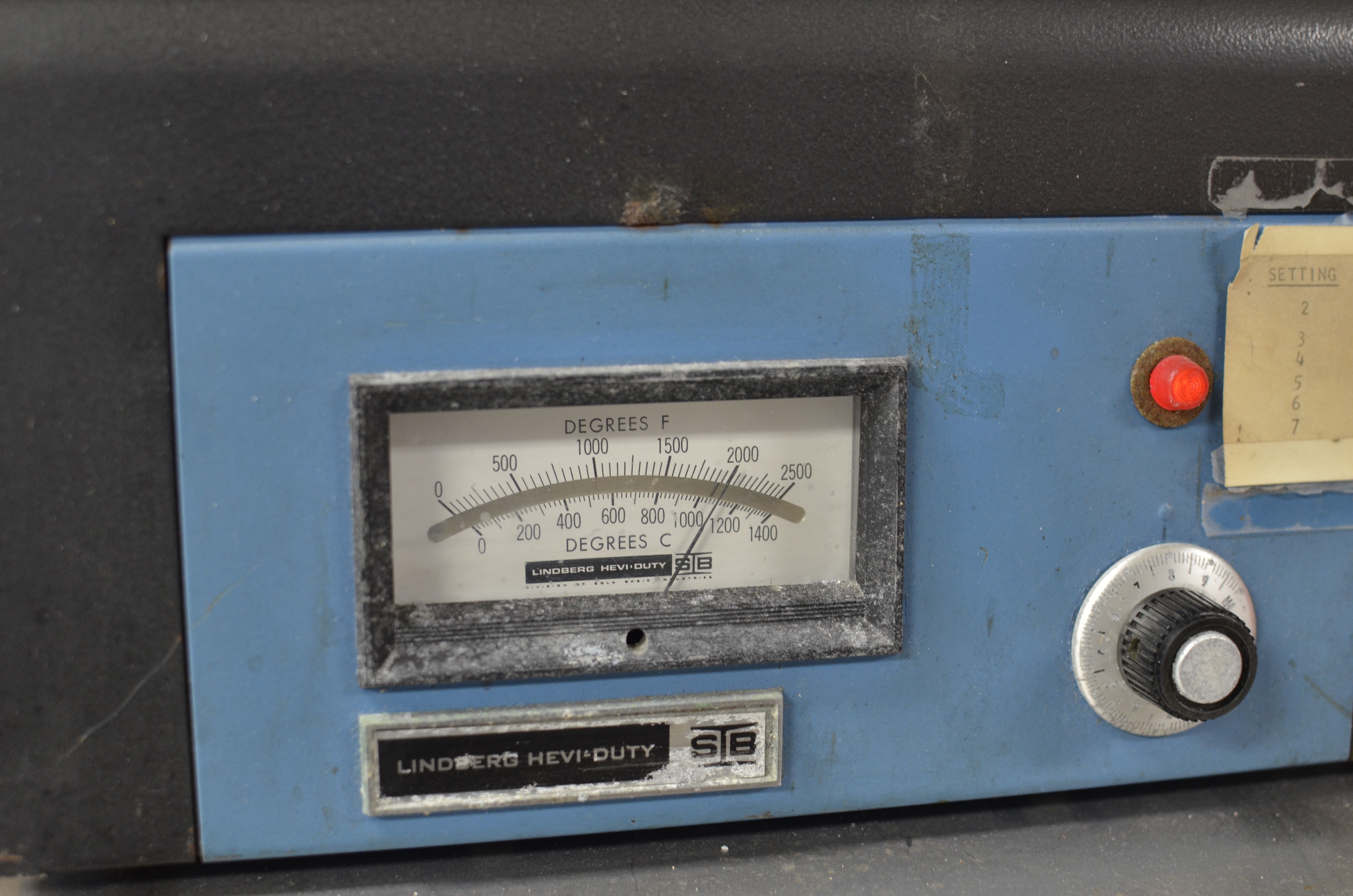
Equipment used in home poly-gate process:
-Hotplate
-Tube furnace
-Lithography apparatus
-Microscope
-Vacuum chamber to deposit metal
Z2 “gate first” process (similar to standard self-aligned process but without a field oxide):


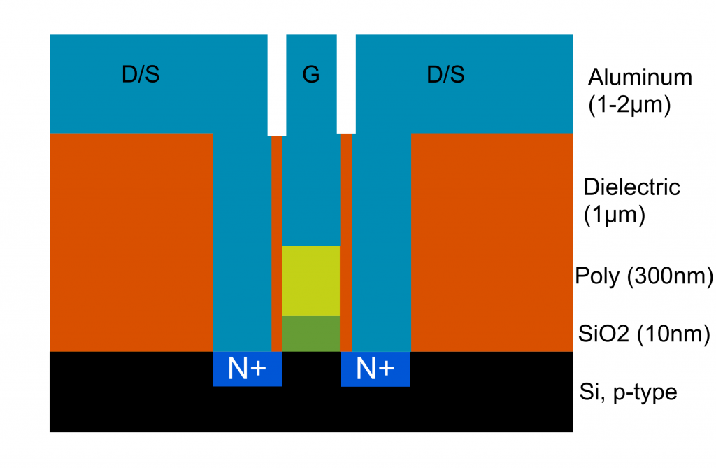
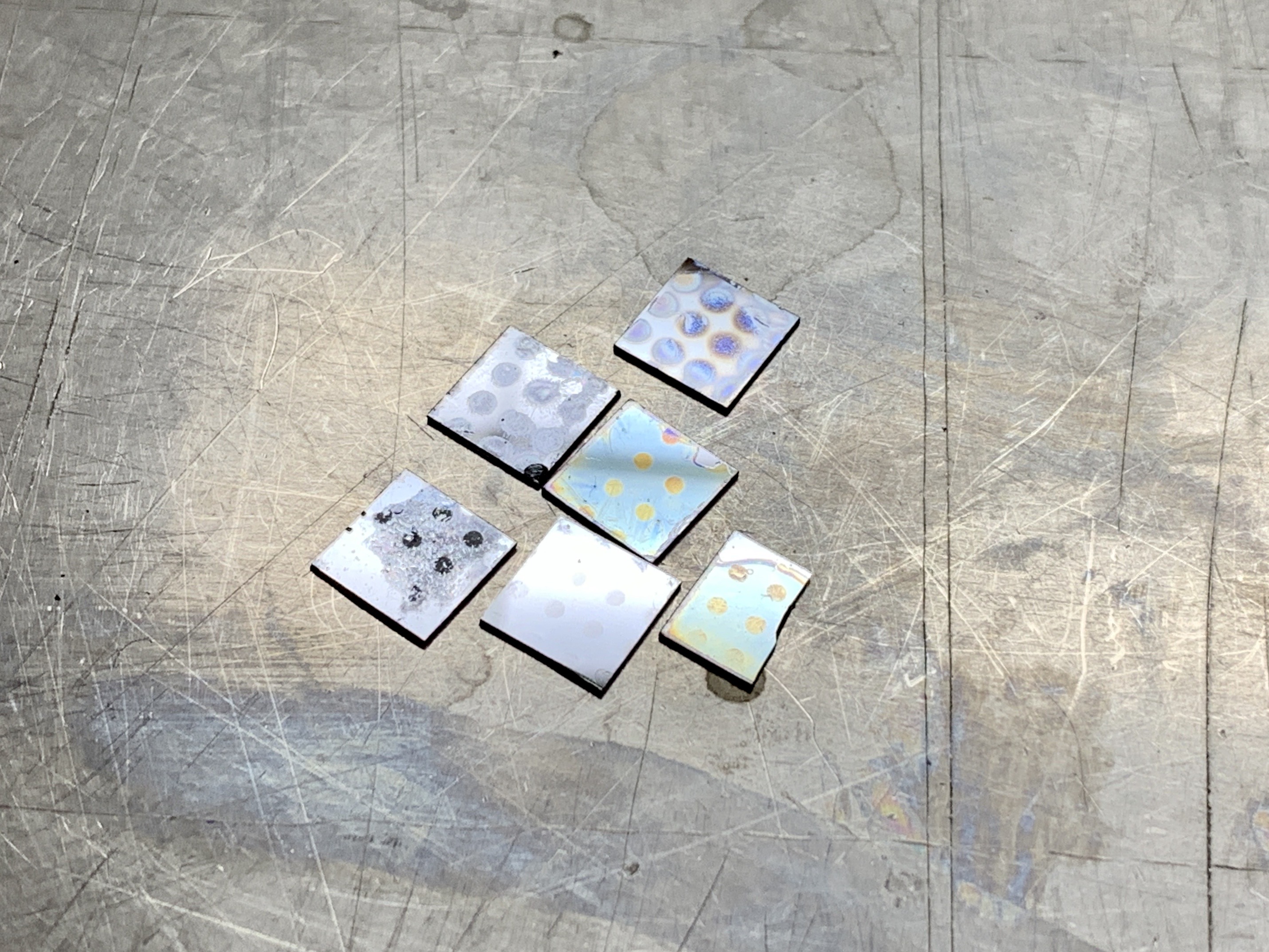
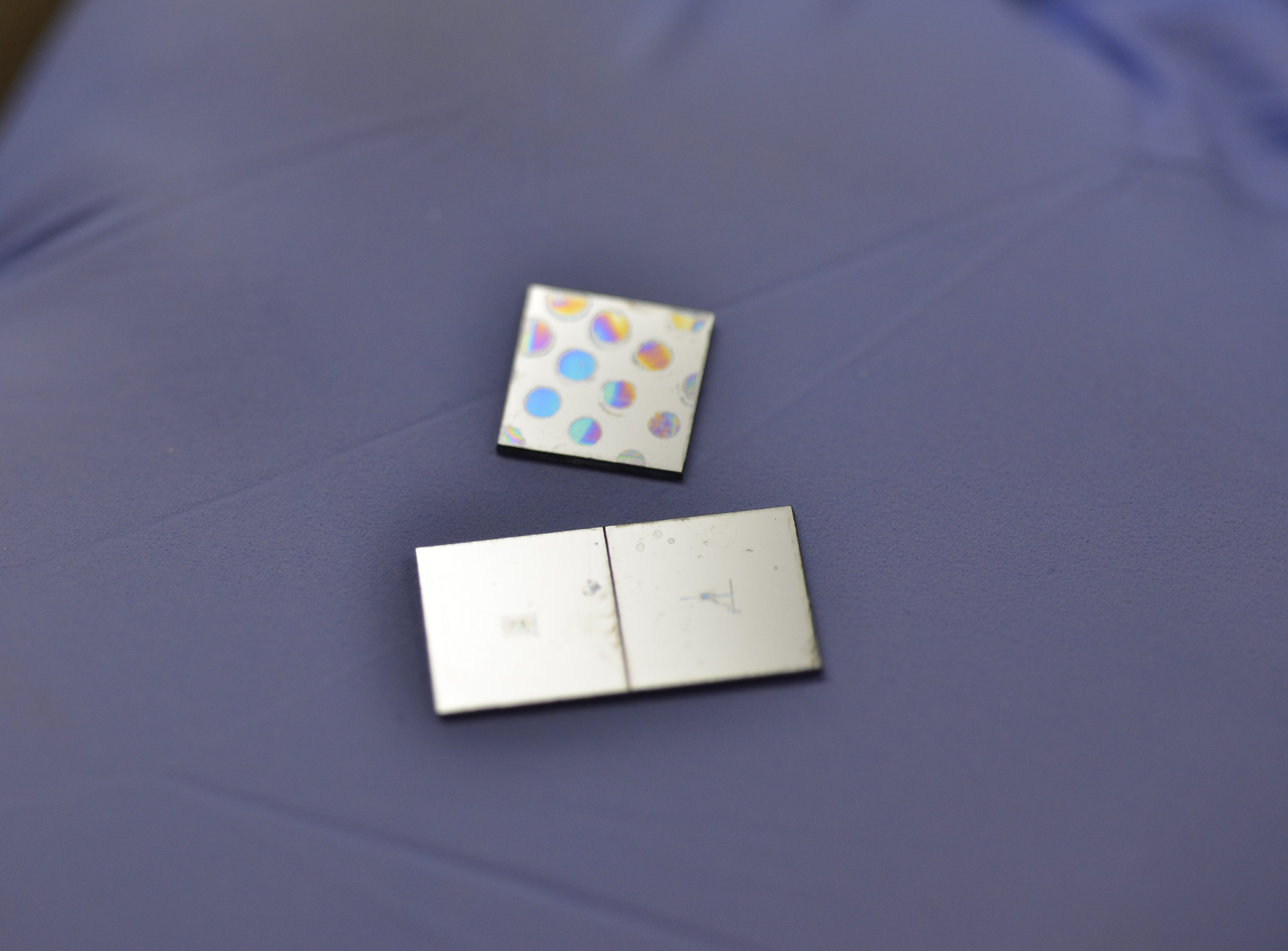
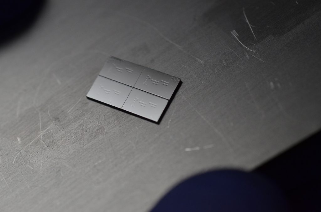
I snapped one of the test chips in half (functional Z2 but with bad layer alignment and thin metal, about 300nm) and put it in my SEM for a cross section:
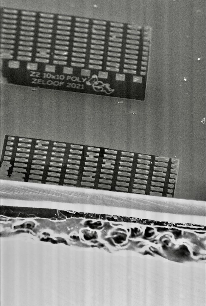
Find the dust particle in the red circle below, use that to get oriented in the coming cross section views.

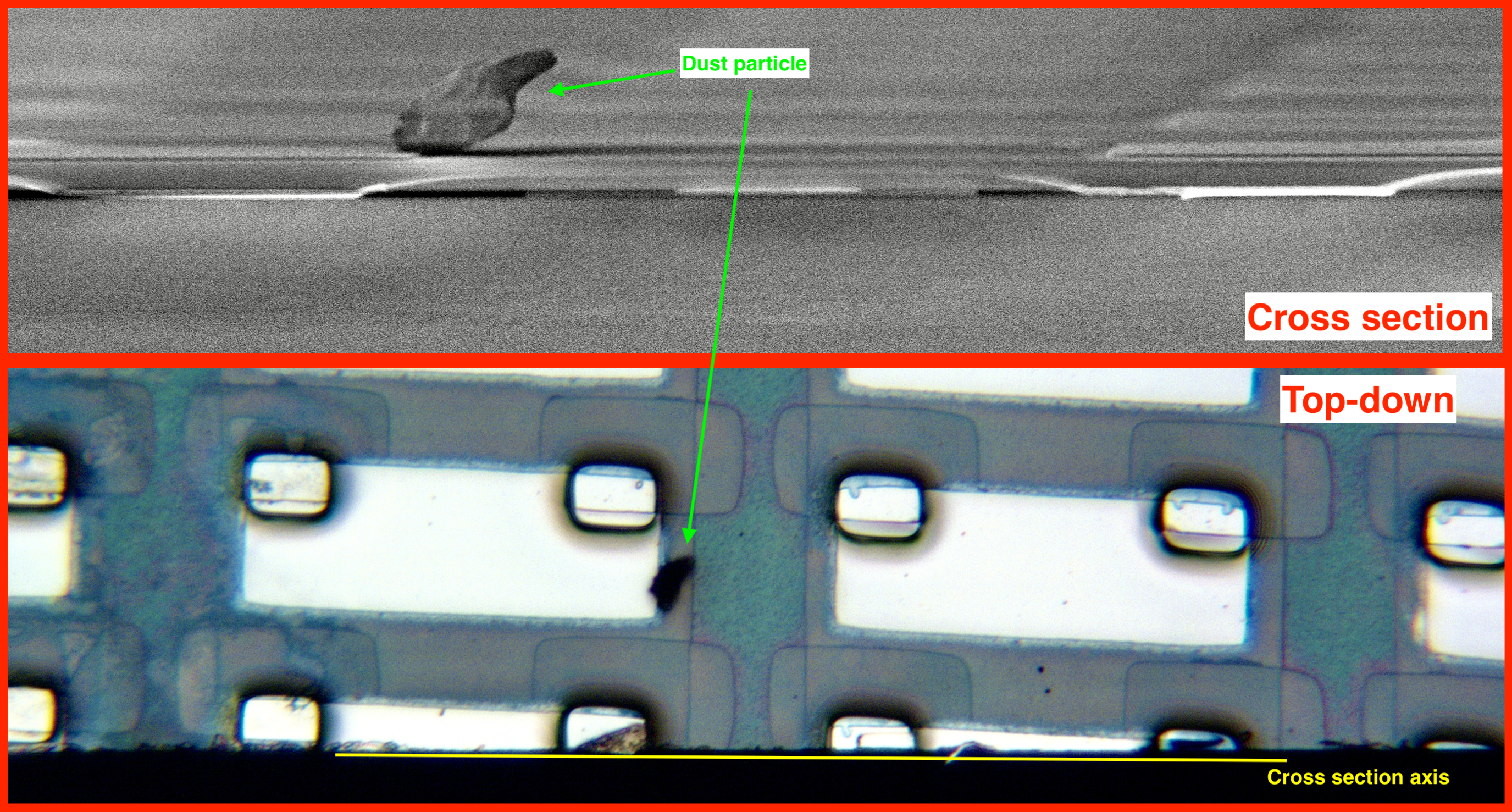

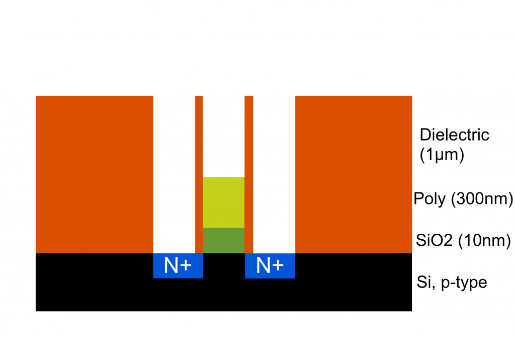
Because I bought the wafer already with gate oxide and polysilicon on it, I can’t grow a field oxide. These thick oxide layers are typically used to mask dopants and require a long high temperature step which would oxidize all of my poly and there would be none remaining. So, my modified process uses an additional masking step (the “gate” mask is typically not found in a self-aligned process) that allows me to use the polysilicon itself as a dopant mask and hard-baked photoresist as the field dielectric. This alternative processing results in the stepped structure you can see in the orange region on the NMOS cross section above. This process subtlety is mentioned here, read this twitter thread.

This process isn’t ideal and I want to make some changes so it’s CMOS compatible but it simplifies fabrication and makes it possible with a minimal set of tools. The 1µm dielectric layer (orange) would ideally be CVD SiO2 (it’s possible to build a TEOS oxide reactor at home) but I used a photoresist instead. Most photoresists can be baked around 250°C to form a hard permanent dielectric layer that is an easy alternative to CVD or PECVD oxide. A spin-on-glass/sol-gel could also be used here. SiO2 etching is done with a buffered HF solution made from rust stain remover or RIE.
Huge composite stitched die image:

Thanks for following my work and feel free to contact me with your thoughts!
***DISCLAIMER*** this project is incomplete and the write-up is intended only to save someone a little time who is attempting to explore this topic on their own. I only spent about 2 weeks working on this during winter break from school and also I did very poorly in the organic chem unit in high school which is the extent of my chemistry knowledge. Major YMMV on this one
1) commercial photoresist is expensive – modern photoresist can be upwards of $8,000 per gallon. And you thought gasoline prices were bad?
2) commercial photoresist is hard to get – even if you can afford it, no actual photoresist supplier will ship (even samples) to an individual or residential address.
So, unless you make friends in industry/academic lab so that your refrigerator looks like mine then it may be impossible for you to do photolithography at home. The good news, however, for making chips at home is that photoresist is the only major chemical that is difficult to source. Everything else can be found in the local supermarket or on sites like eBay/Amazon (rust stain remover HF, boric acid roach killer, etc.) This means that if a reliable synthesis method for photoresist is found, making ICs at home will become one step more accessible.

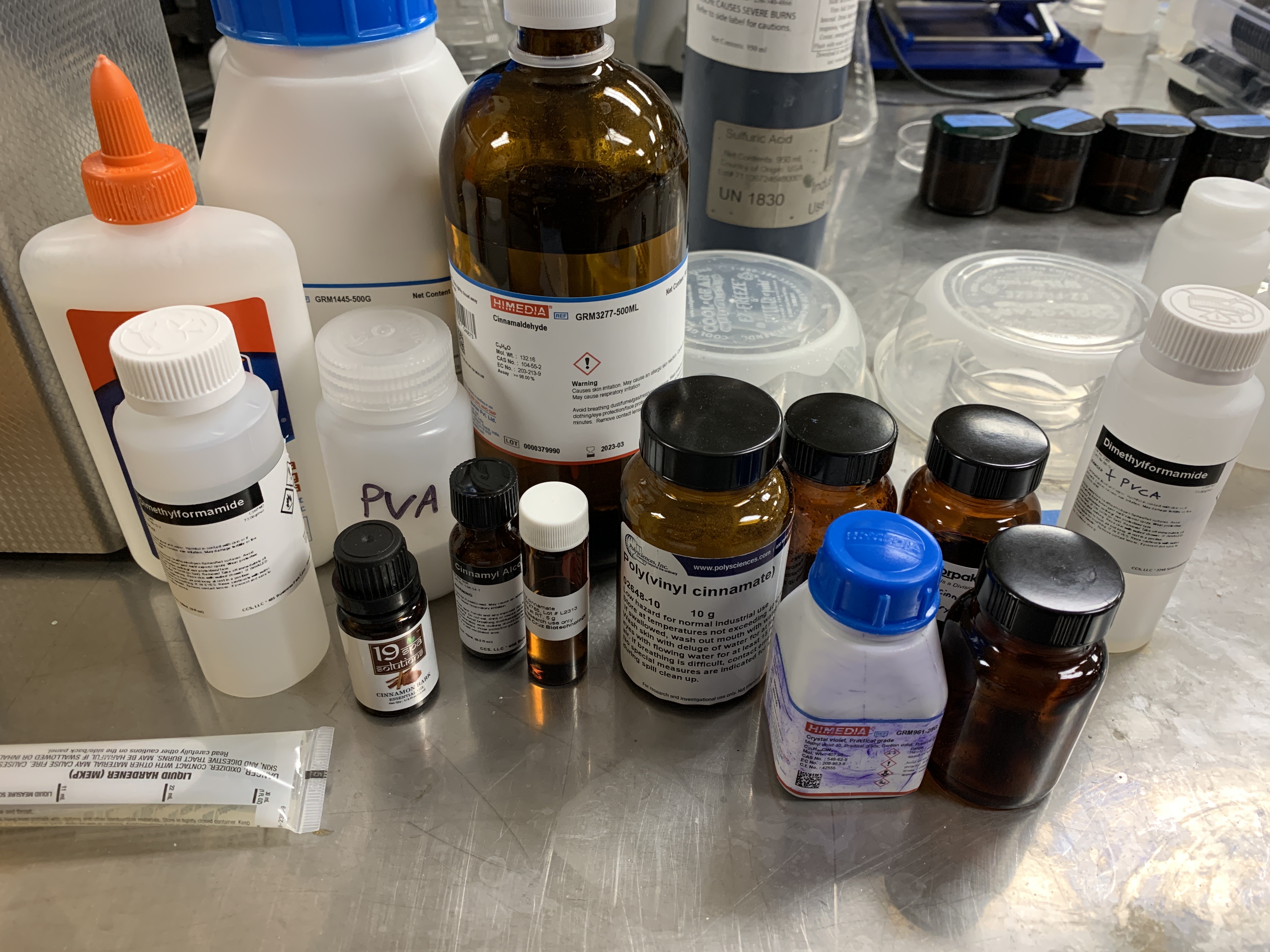
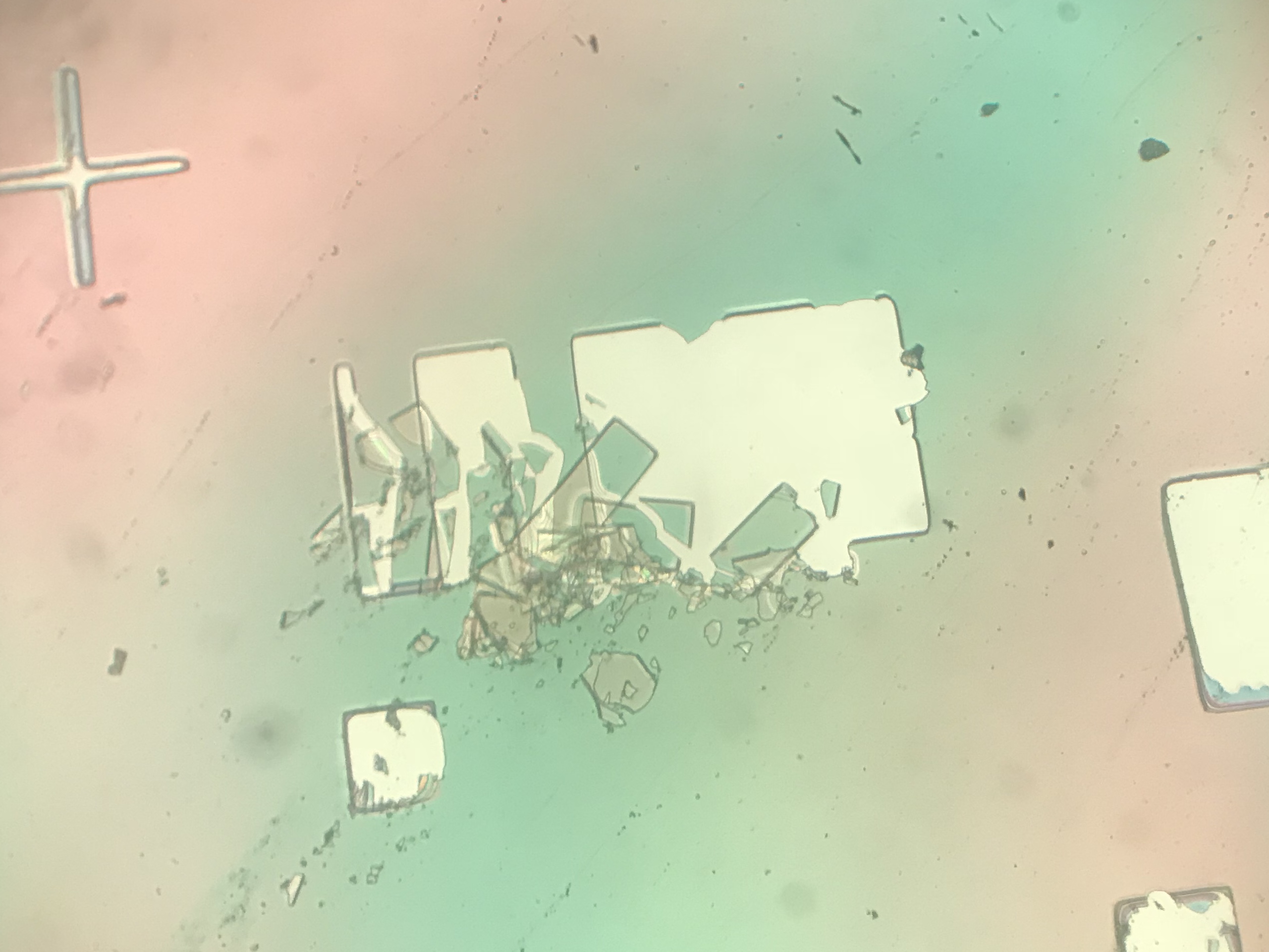
In the 1950s, Dichromated gelatin was a contender for the first “photoresist” for early microelectronics, but it couldn’t withstand more than ~1% HF etching solution. Also, it had a “dark reaction” in which it would decompose readily without use. So, early IC pioneers at Bell Labs teamed up with the smart people at The Eastman Kodak Company and came up with poly(vinyl cinnamate), an alternative which has no “dark reaction”, excellent chemical stability, and relative ease of synthesis. Also, most of the chemistry smells very good for this because it is based on cinnamon-like compounds. However, poly(vinyl cinnamate) was quickly replaced by cyclized rubber resists because of its superior adhesion to Silicon. For this project, I have chosen to try synthesizing poly(vinyl cinnamate) because it is the easiest and requires the least precursors with above a 3 on the NFPA health diamond. Poly(vinyl cinnamate) is a negative acting resist in which the exposed regions become crosslinked an are no longer soluble in the developer solution.

For the synthesis, I used <$50 of glassware from Amazon including a Buchner funnel, filtering flask, and assorted small beakers. A hotplate with stirrer is nice. All of the following chemistry should be done in subdued room light, without any natural light from the Sun. Most interior LED lighting will not expose these materials for a matter of hours and are safe to work under, it definitely does not need to be carried out in darkness.
Supplemental readings on Poly(vinyl cinnamate) synthesis:
Photochemical properties of cinnamic acid epoxy esters
Original Kodak patent on its synthesis and use

Directly after spin coating, all samples are soft baked at 50ºC on a hotplate for 1 minute. Then, the poly(vinyl cinnamate) films were exposed using an unfiltered Mercury vapor arc lamp (sunlight works too!) in the form of a Loctite UV epoxy curing lamp. For order-of-magnitude exposure dosage calculations, this lamp has an approximate intensity of ~80mW/cm^2 at the 365nm emission line. Proper poly(vinyl cinnamate) films can be exposed in a matter of seconds with this. To yield a visible image, the samples are developed in MEK for about 1 minute which concludes the photolithography process.
Continue reading DIY Photoresist – Notes on Poly(vinyl cinnamate) synthesis
Homemade Silicon MEMS
The term MEMS was first coined in the 1980s and has since brought tons of innovative/insane fabrication techniques and incredible devices. Among my favorite examples of this is the DLP technique invented by TI and a DNA nanoinjector for cells made at BYU (pictured below). Obviously, I won’t be making anything this complicated but had some decent results on my first attempts that are worth sharing and continuing to work on.

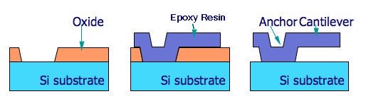
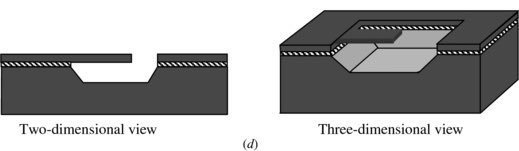
All of my MEMS devices are fabricated with chemical etching and maskless photolithogrpahy. The most basic free-standing mechanical device is the cantilever, which can be made using a sacrificial underlayer made of oxide or photoresist (SiO2 in my case) and a harder upper layer (SU-8 epoxy resist in my case) which remains when the sacrificial layer is removed with chemical etching (HF for SiO2). These can be made into oscillators, nano balances, any many other useful instruments.
There are many variables here to optimize, so it is best to run many experiments at once.


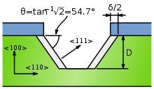
The next MEMS technique to demonstrate is bulk Silicon Micromachining which leverages the high level of order in a monocrystalline Silicon wafers to make controlled and often self-terminating etches. On a standard <100> orientation wafer, a solution of KOH (KOH pellets from amazon/ebay dissolved in water) can anisotropically etch Silicon to expose the <111> crystal face at at an angle of 54.7º from the wafer surface.

The setup for this is quite simple, 60% KOH solution with a dash of isopropyl alcohol is brought to 80°C in a hotplate with stirring and etches about 90um in 1hr, or about one-third the thickness of a Silicon wafer. Nature’s fume hood is used for this experiment.
A top layer of SiO2 is used as a hard mask to etch the underlaying Silicon. Before KOH etching, the SiO2 is thermally grown and patterned in a standard process by maskless photolithography and HF etching. The active layer mask for my Z1 amplifier chip was used here as a quick and convenient anisotropic etch test. Wafers are then inspected under SEM.
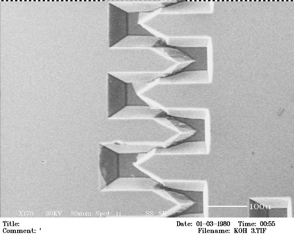


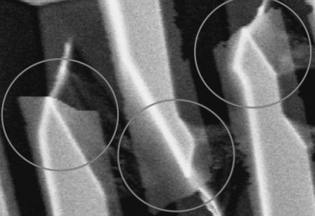
Suspended cantilever-like structures can also be made here. The first KOH etching attempt shows some undercutting, but in the future stirring conditions will be optimized to provide more undercutting. The circled areas in the high-tilt angle SEM image below show 500nm thick SiO2 overhanging 90um of airgap above the Silicon surface.
Homemade Memristors
Memristors are interesting devices first posed by Leon Chua in 1971 as the 4th basic circuit element, after the resistor, capacitor, and inductor. It would theoretically satisfy a relationship between charge and flux, and in simple terms is a 2-terminal device whose instantaneous resistance depends on the device’s electrical past (total charge or current that has flowed through the device). The possibility for existence of a memristor in our universe is highly debated and claims of “discovering” the missing memristor were circulated by HP Labs in 2008. The resistance-memory effect they noted was met with huge amounts of press and recognition, but in reality it was first noted in the late 1960s in similar materials and was not valid under the original mathematical definitions for a memristor. Since then, the definition and requirements for a memristor have been relaxed by some and even Leon Chua himself has recognized HP’s memristor. As with most politics and similar situations in academia, you should read about this on your own and come to your own conclusions, but it is safest to describe such devices with a resistance-memory as “memristive devices” or “memristive systems”, because while they may not adhere to the original definition of a memristor, they are still worth exploring and have proved to be useful for machine learning and artificial neuron applications. Interestingly, an ideal memristor fits as a perfect electrical model for Axons/synapses.

Most of these memristors are made with some metal oxide stack with top and bottom electrodes and rely on the electrical current moving oxygen vacancies within the metal oxide to create a sort of hysteresis in resistivity. The results in a unique pinched-figure-eight hysteresis type IV curve whose loop area decreases with increasing frequency:

Basic memristive devices can also be made easily at home out of Copper Sulfates, as described here and here. Of course, it is advantageous for lots of reasons to be able to manufacture these on a parallelized, industry standard CMOS-type fab process, where thousands of these devices can be made at once using photolithography.
About 2 years ago when I was setting up my sputtering chamber, none of the coatings were conductive. This was frustrating but eventually I figured out the films were metal oxides, not pure conductive metal coatings, due to too much Oxygen being present during the sputtering. Recently, I read that memristive devices can be made out of materials such as Titanium and Copper oxides, so I dug out some old failed sputtering attempts of these materials, put them back in a chamber to deposit a top Copper electrode, and measured their IV characteristics.

Both Titanium and Copper oxide based devices worked as memristive systems and showed similar characteristics. The bottom electrode in both cases was doped Silicon which causes the devices to be slightly rectifying (asymmetry in curve) and highly sensitive to light (built-in PN junction) but they still show a resistance-memory hysteresis effect. In the future, more devices will be built on insulating substrates and should yield much better results. Rectifying memristors made on Si substrates have applications in high density 3D array stacks, even though they deviate highly from an “ideal” memristor.


Figure (a) above shows a typical curve from one of my devices and figure (b) shows a curve from a paper published studying similar metal oxide-based memristors. Scale on fig. (a) is 100uA and 5V per division.

Here, differences in slope (1 / resistance) for the on (blue) and off (red) regions can clearly be seen, as well as the switching region (yellow).
As previously mentioned, these devices are highly light-sensitive due to the doped Si substrate and a have very strange response:
After these first encouraging results, I made Copper Sulfide based devices that actually exhibit more ideal characteristics and can be made for a few dollars. Excess pure Sulfur powder from Amazon is dissolved in Ethanol or Isopropyl alcohol and a bare Copper PCB was placed in solution for 12 hours. The experiment was in a closed vessel to avoid evaporation and a black CuₓSᵧ film was noted. Then, the device was washed in alcohol for 3 hours to remove any residual Sulfur particles before being probed with a function generator and oscilloscope wired as a curve tracer.
Homemade CuₓSᵧ memristors:
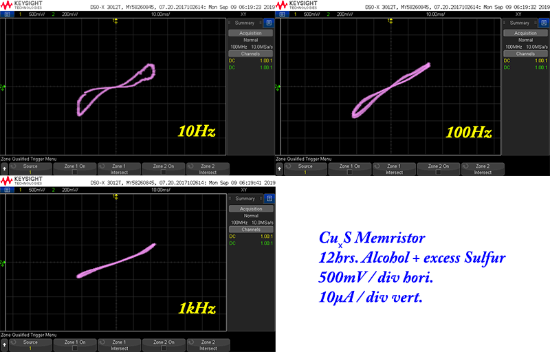
A nice figure-eight is seen to pass through the origin and have a loop area which is decreasing with increasing frequency, as expected by the equations that govern a memristor (time integral of charge or current).
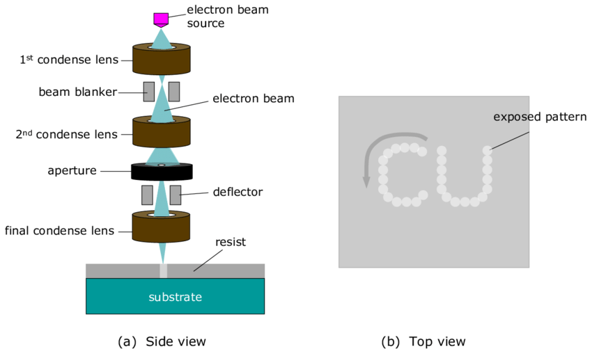
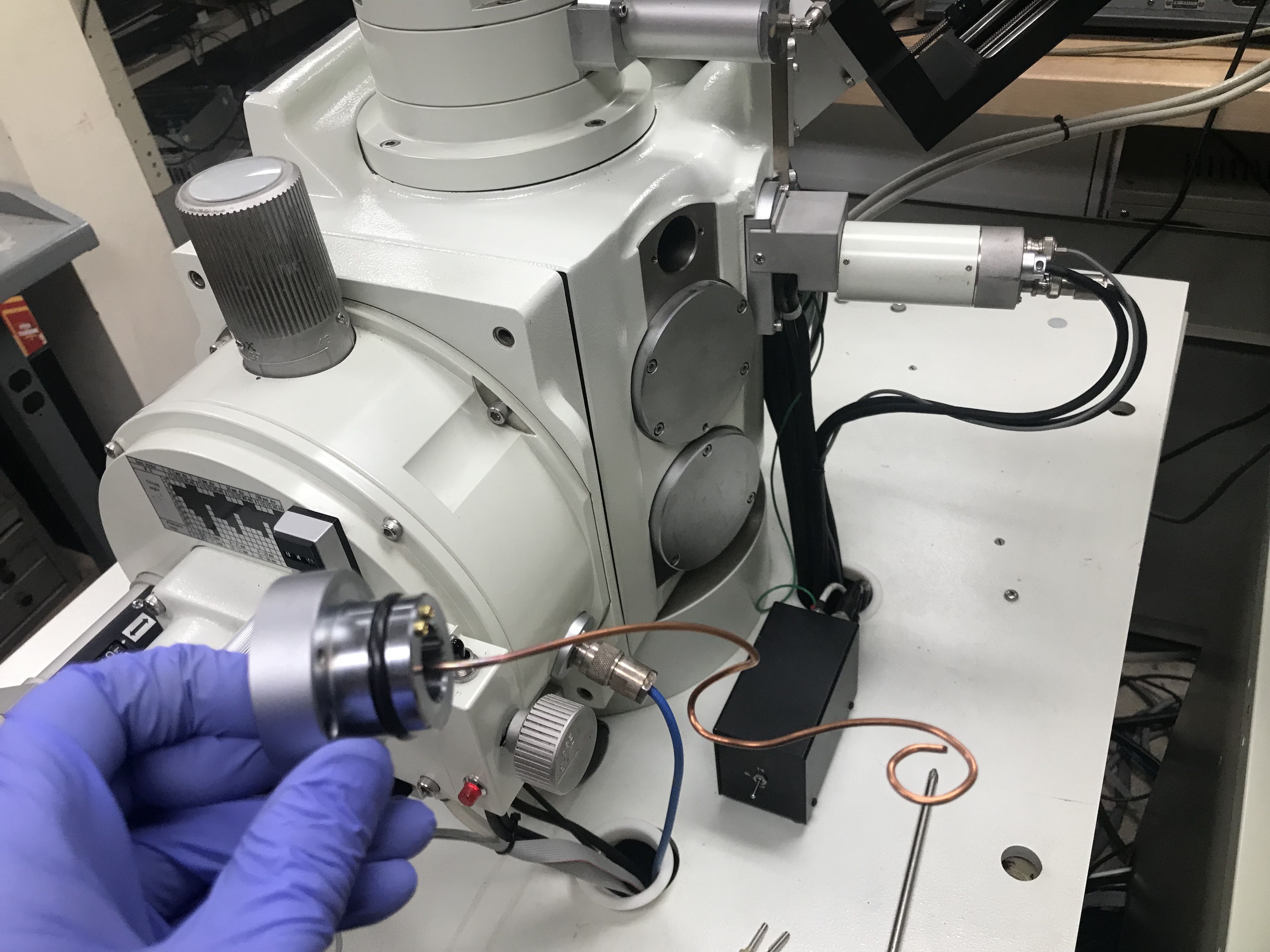
I modified my JEOL scanning electron microscope to not only image tiny things, but make tiny things too.

This technique is called Electron Beam Lithography. Normally, a SEM works by scanning a beam of electrons over the sample and detecting secondary electrons. In this case, I built a PC scan controller that “drives” the electron beam around and draws the image onto the sample which is coated with electron-sensitive resist.
 For resist, I used SU-8 although PMMA (Acrylic) dissolved in solvent will work as well.
The scan controller uses dual 12 bit DACs. They had current outputs so a transimpedance amplifier creates +/-10v proportional to that current to drive the microscope’s external XY inputs. The controller also contains an Arduino and Altera CPLD. To turn the beam off when needed, a high voltage is generated (+2kv) and applied to a “beam blanker” inside the microscope.
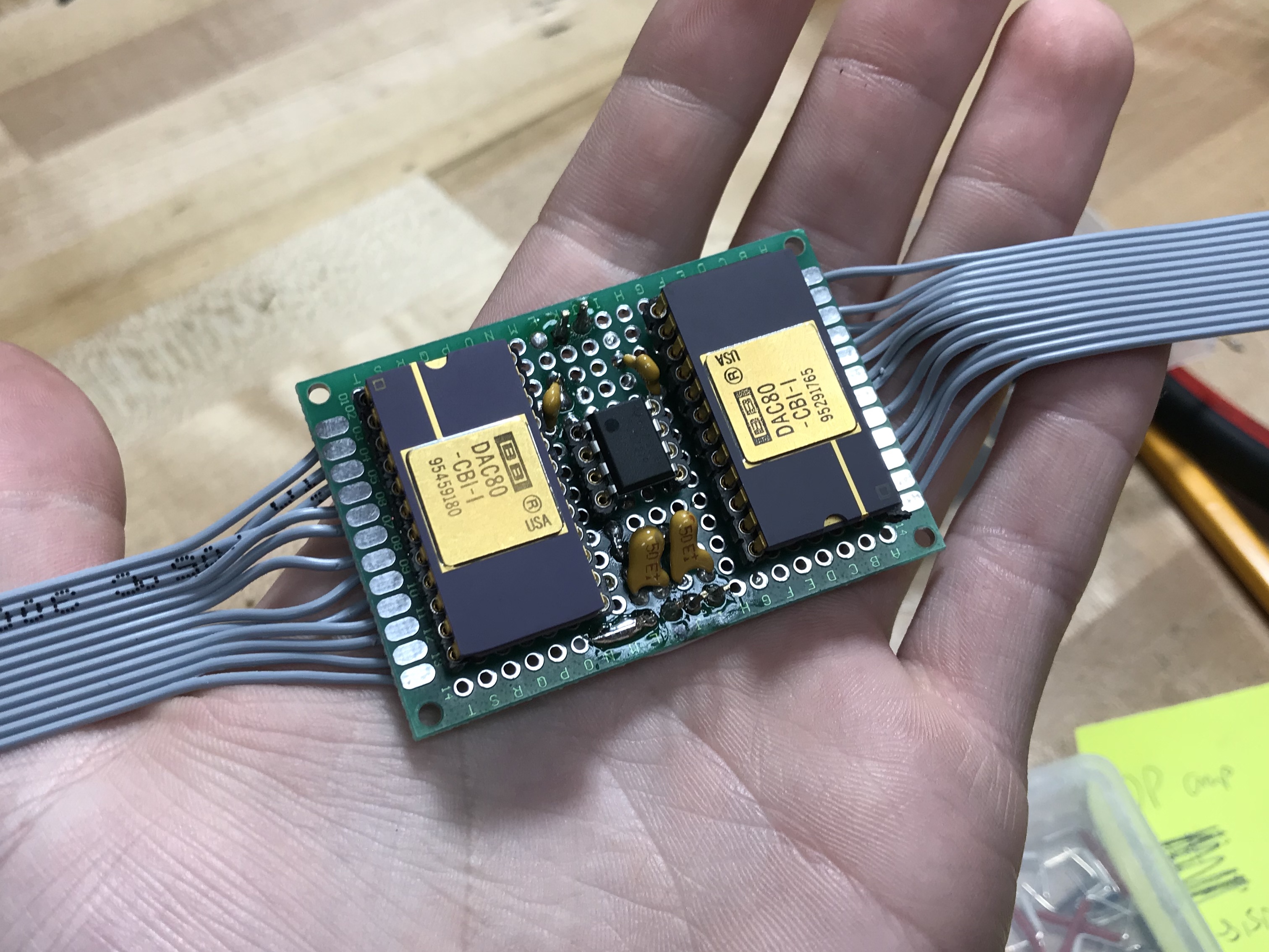


I learned that the 12 bit DACs do not nearly have enough resolution, so I will be looking at upgrading to at least 18 bits hopefully. Also, the geometry of the beam blanker is not correct to create a high electric field in its center, so the beam is only partially de-focused and never fully “turns off”.
Update (2020): New photos with improved beam blanker –


This project involved developing a sputtering system in collaboration with Ilya Drozdov in the Oxide Molecular Beam Epitaxy / Condensed Matter Physics Group at the Brookhaven National Laboratory. This system has 2 process gas feeds, an infrared substrate heater, and is designed for low-rate coatings that last 2 weeks each.
You can see other services that I offer here

The vacuum system consists of a large dual turbo pump (510L/s) backed by a scroll pump and throttled with an 8″ VAT gate valve. The process requires O2 and Ar lines on Mass Flow Controllers plumbed in as well. The MKS controller drives the MFCs to flow in the process gasses in the correct ratios and keep the pressure within 1% of the setpoint.


The chamber is quickly evacuated to the 1e-7 Torr range although the actual process occurs around 50 – 100mTorr under O2/Ar atmosphere.
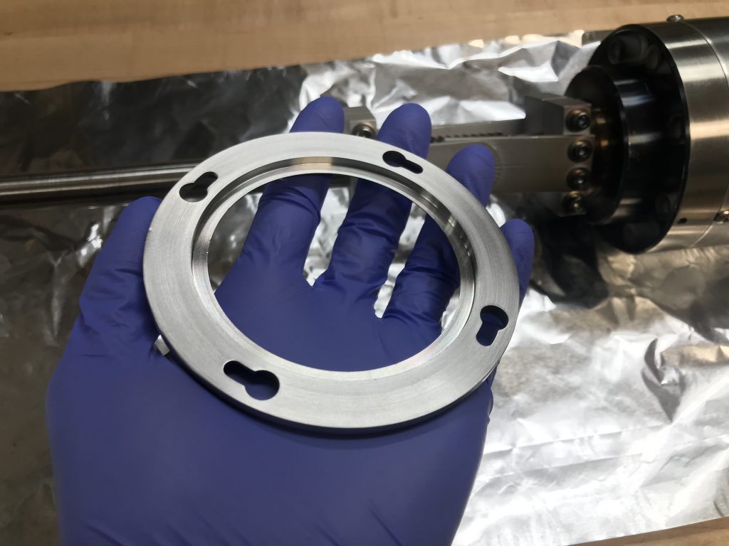
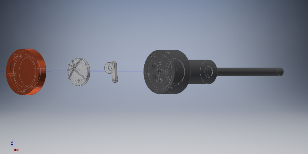
The 3″ dia. sputter gun was salvaged from combining old stock of broken ones together and making one functioning sputter gun.
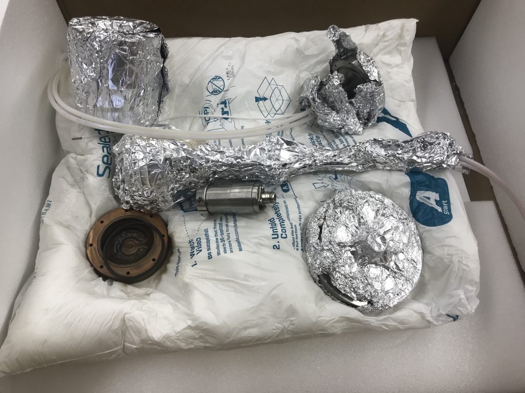
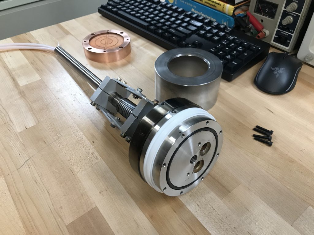
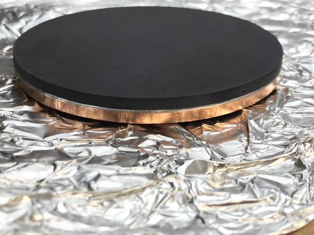
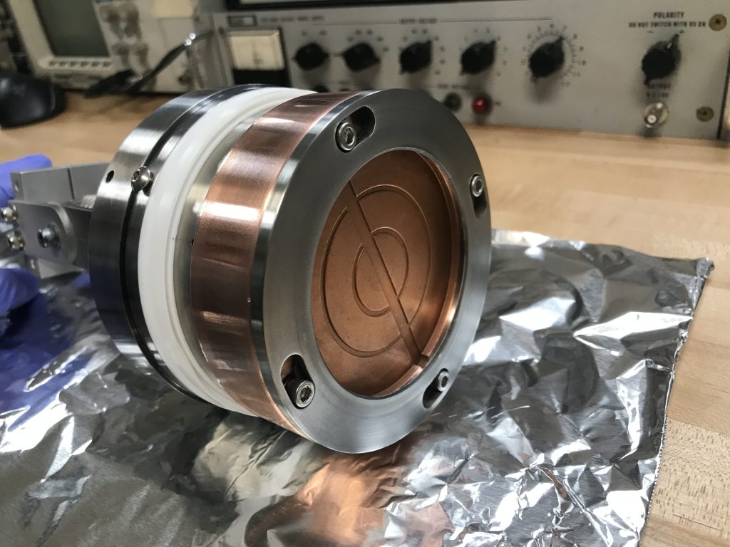
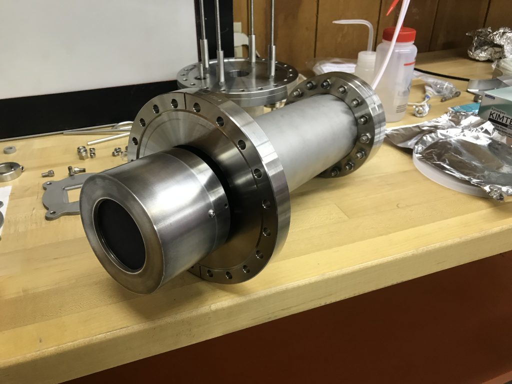
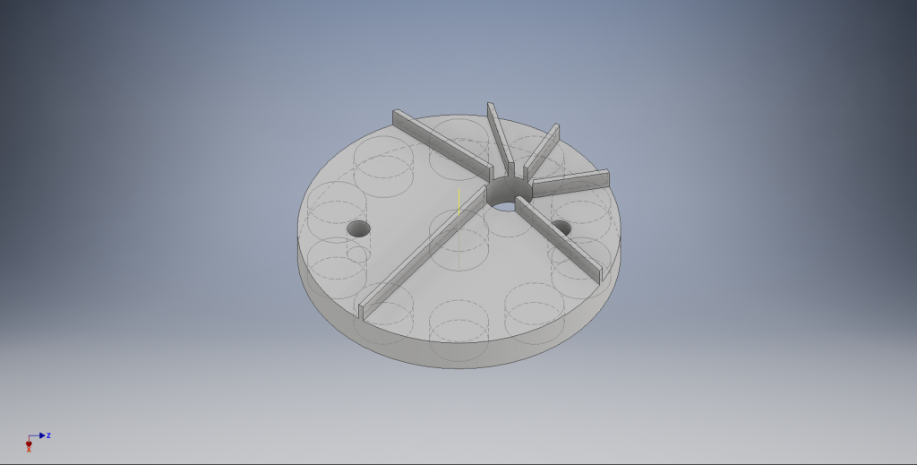
The sputter target is clamped to the Copper puck which is water cooled because of the high power involved in these sputtering processes. All of the sputter gun parts I started with had rusted magnet assemblies, so I had to make a new one. A 3D printed puck that fits inside the copper piece was designed with embedded rare Earth magnets to create a surface DC field of around 400 Gauss which confines electron movement and induces the magnetron effect.
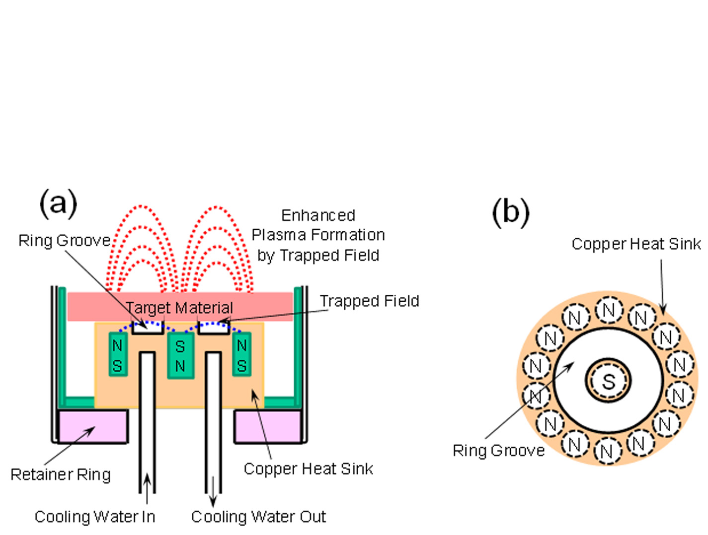
The “racetrack” ring-like plasma density in front of the target indicates the circular path of the electrons due to the Lorentz force, meaning that the magnet assembly has sufficient strength at the surface of the target.

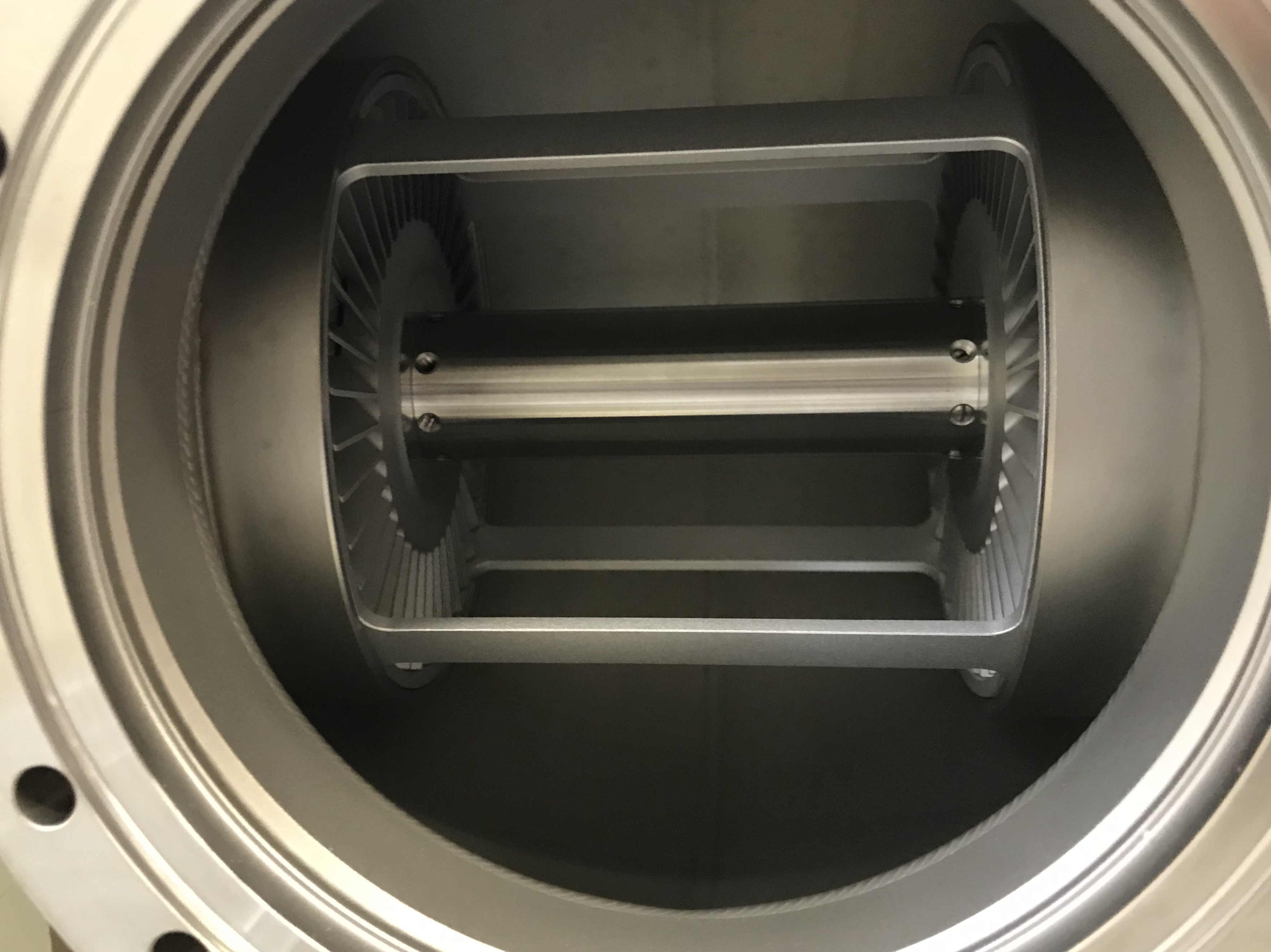
The final part of the project was the substrate heater which heats the sample from the back while it is being coated from the front. The specific process required that the substrate to be at elevated temperature (up to 850C) for 2 weeks. An infrared substrate heater was designed using 300W USHIO quartz lamps and a water cooled Aluminum parabolic reflector to focus the light onto the substrate.


All parts of the heater which are exposed to elevated temperature are made from Inconel to avoid contamination of the delicate experiments. This includes the thermocouple, which is sheathed in Inconel and the wires are braided in Inconel as well.


In IC fabrication it is necessary to deposit/grow and etch insulating layers of Silicon Dioxide. This presents a few problems for standard photolithographic patterning because SiO2 is hydrophilic which can cause photoresist adhesion issues and also the HF etchant attacks most photoresists. These issues combine to leave you with poor pattern definition and often complete photoresist lifting during etch.


The steps I have found to mitigate these issues are (in order): dehydration bake, HMDS vapor prime, thick resist coating, hard bake, and buffered oxide etch.
First, SiO2 is thermally grown on a test wafer using a water vapor source on a nearby hotplate to fill the furnace with steam during oxidation. The first step to ensure good resist adhesion is a dehydration bake which creates a hydrophobic wafer surface. This does not need to be done if the wafer recently came out of the furnace but if it has been in storage, then a bake of up to 700C may be necessary to restore the dehydrated surface. The next step is HMDS vapor priming:


Here, the wafer is heated to around 200C in the presence of Hexamethyldisilazane (HMDS) vapor forming a surface monolayer on the wafer that further increases resist adhesion. HMDS can also be spin coated but this often yields a far too thick layer and can lead to incomplete photoresist development.
The final steps before etch are to spin the resist and to hard bake it. Naturally, a thicker resist film allows for a longer etch time. For maximum chemical stability, the hard bake should be conducted for extended periods of time close to the resist softening point which is usually around 145C. This can make the photoresist difficult to remove, so an ultrasonic acetone bath may be necessary unless you have proper stripping chemicals. If difficulty persists, then it is likely that the top layer of resist has cross-linked and you may be unable to remove it. One may try high power Oxygen RIE followed by Piranha solution and N-Methylpyrrolidone (NMP) stripper as is used commercially to remove resists after hard ion implantation.


Instead of a standard HF etch, a buffered oxide etch of NH4F (Ammonium Fluoride) in HF can be used to control the etch rate and photoresist lifting. I use approximately 20-30g of 100% NH4F per 50mL of HF (stock whink rust remover) and etch time for 6000Å SiO2 is 20min at 20C. A couple drops of Triton X-100 nonionic surfactant may be added to the BOE to improve etch uniformity, wetting, and ensure consistency through a thicker resist. A good BOE recipe can be found here but assumes industrial-strength HF.


Etch trials
Homemade computer chips / integrated circuits
I am very excited to announce details of the first homemade integrated circuit and share the journey that this project has taken me on over the past year. I hope that my success will inspire others and help start a revolution in home chip fabrication. When I set out on this project I had no idea of what I had gotten myself into, but in the end I learned more than I ever thought I would about physics, chemistry, optics, electronics, and so many other fields. Furthermore, my efforts have only been matched with the most positive feedback and support from the world; I owe a sincere thanks to everyone who has helped me, given me advice, and inspired me on this project. Especially my amazing parents, who not only support and encourage me in any way they can but also give me a space to work in and put up with the electricity costs… Thank you!
Let’s democratize the tools of innovation.
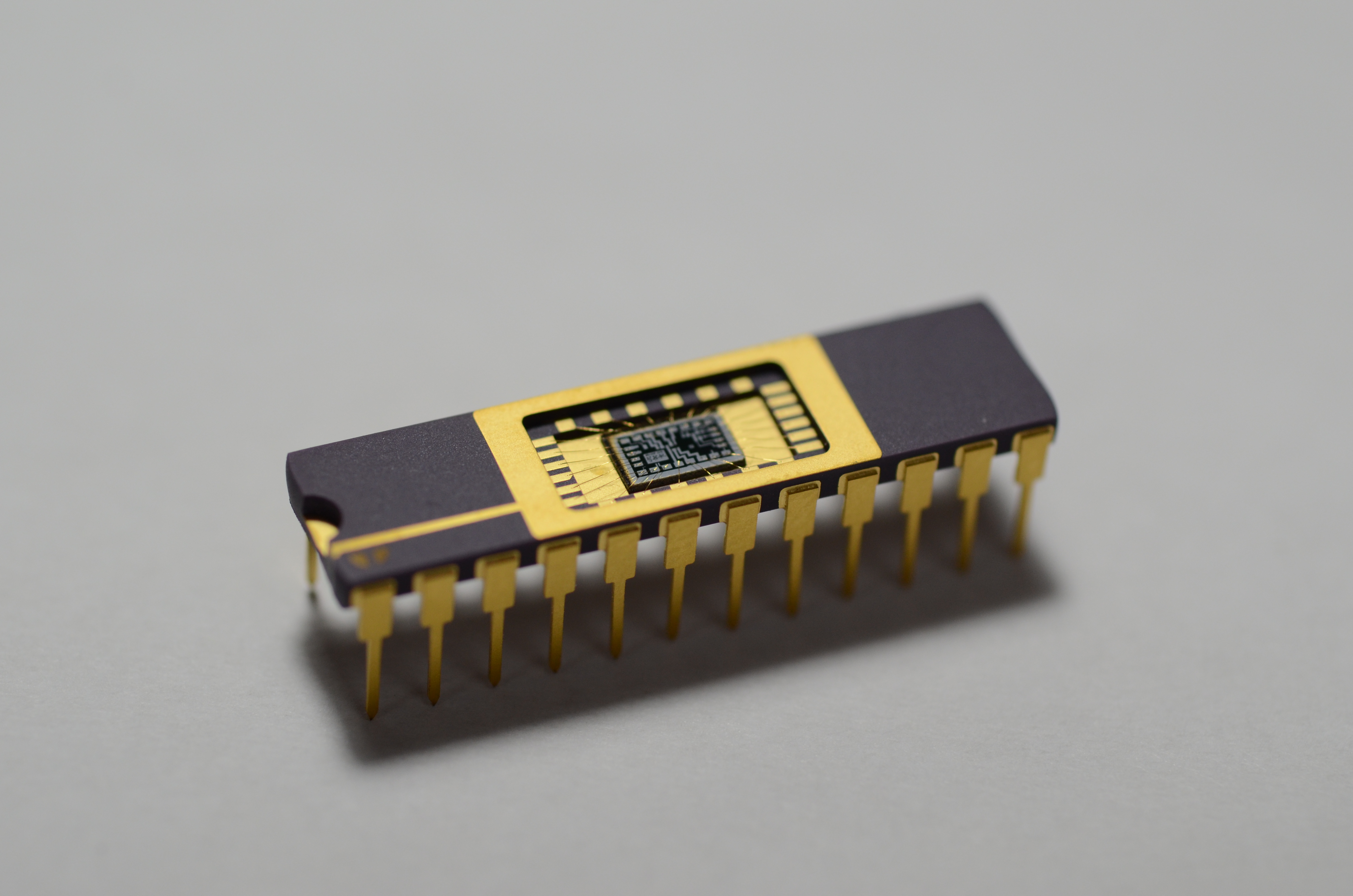 I present the first homemade (lithographically-fabricated) integrated circuit – the “Z1” PMOS dual differential amplifier chip. I say “lithographically-fabricated” because Jeri Ellsworth made the first transistors and logic gates (meticulously hand wired with conductive epoxy) and showed the world that this is possible. Inspired by her work, I have demonstrated ICs made by a scalable, industry-standard, photolithographic process. Needless to say, this is the logical step-up from my previous replication of Jeri’s FET fabrication work.
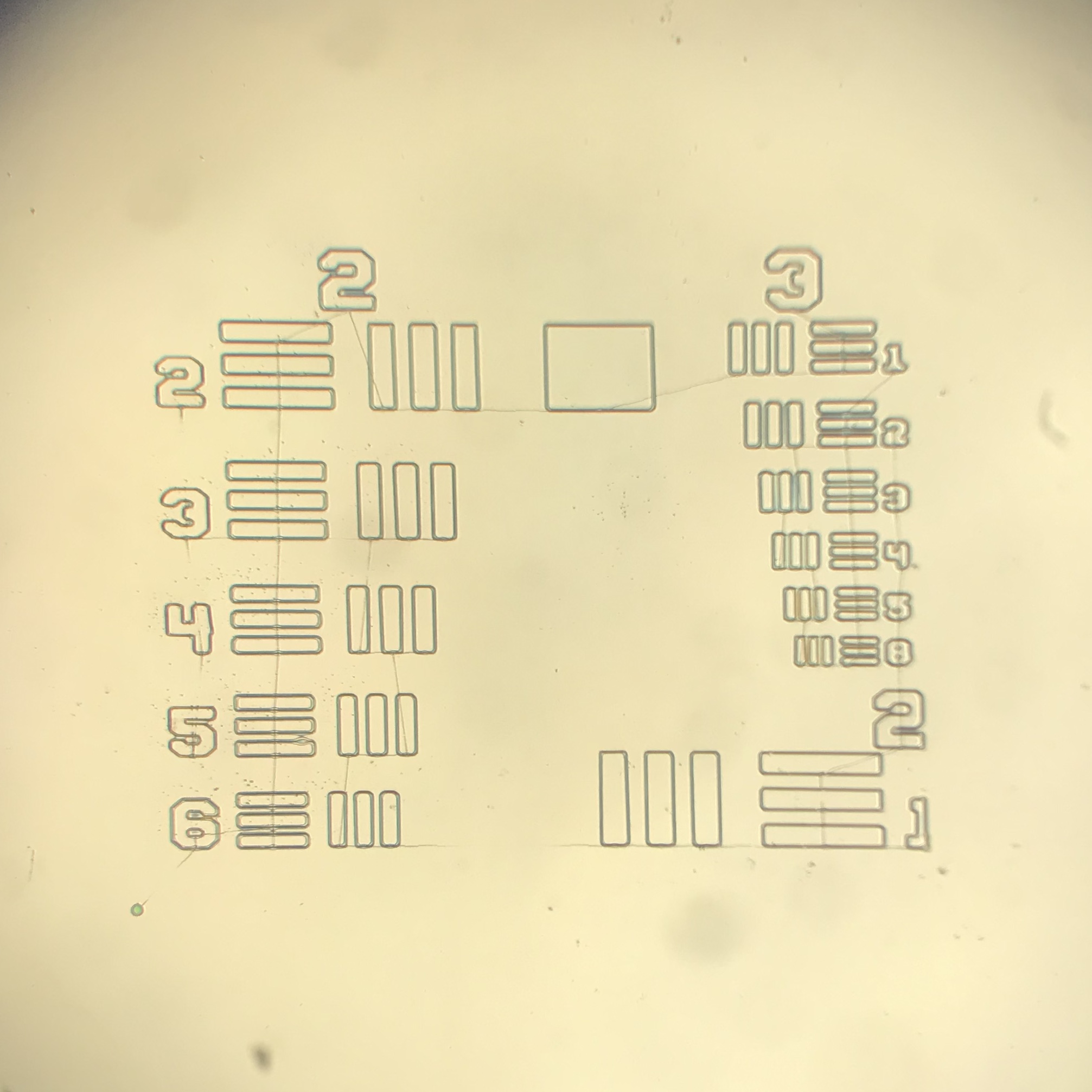
I designed the Z1 amplifier looking for a simple chip to test and tweak my process. Layout was done in Magic VLSI for a 4 mask PMOS process (active/doped area, gate oxide, contact window, and top metal.) PMOS has advantages over NMOS as far as mobile ionic contamination that lends it to being fabricated in a garage. The masks are designed in 16:9 aspect ratio for easy projection.


The feature (gate) size is approximately 175μm although there are test features as small as 2μm on the chip. Each amplifier section (center and right) contain 3 transistors (2 for long-tailed differential pair and one as current source/load resistor) which means a total of 6 FETs on the IC. The left portion of the IC contains resistors, capacitors, diodes, and other test features used to characterize the fabrication process. Each node of the differential pairs is broken out to a separate pin on the lead frame so it can be analyzed and external biasing can be added as necessary.

EDIT: see update at the bottom, the transistor gate length has been reduced to <5µm (1975 tech. level) which brings an increase in device performance.

There are 66 individual fabrication steps to make this chip and it takes approximately 12 hours for a full run. The process yield can be as high as 80% for these large features, but is largely dependent on my coffee intake that day. I have also made Youtube videos covering semiconductor fabrication theory and discrete MOSFET fabrication.
The home chip fab chemistry bench is pictured below and basically includes everything needed to manufacture ICs except a vacuum chamber and a lithography setup. More information about equipment and chemicals is in my Supercon talk from 2018.


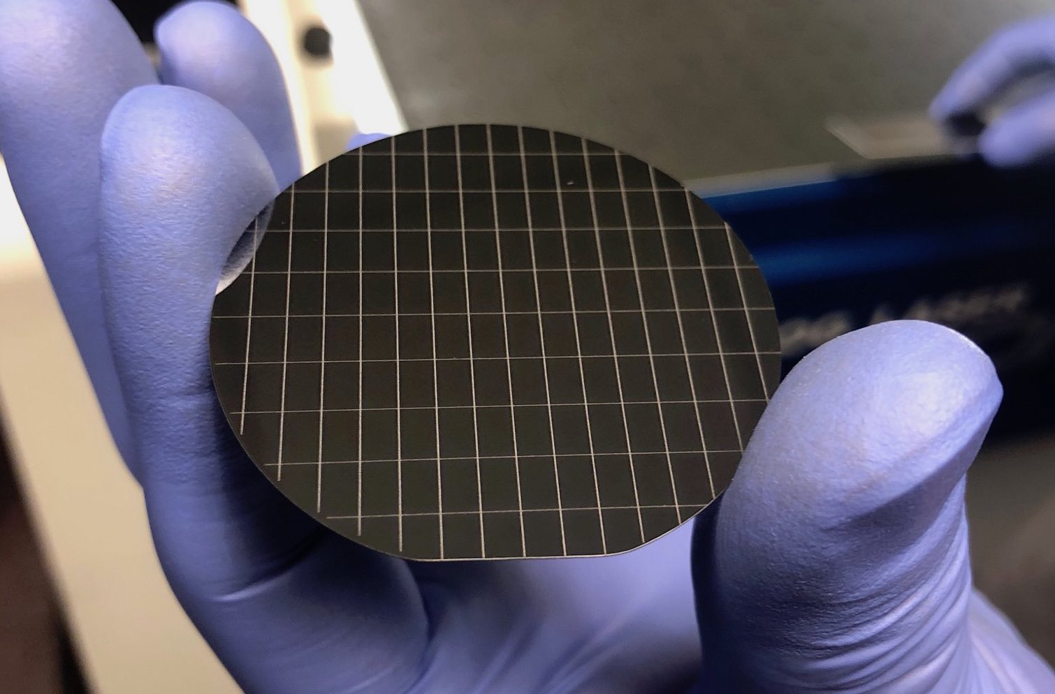
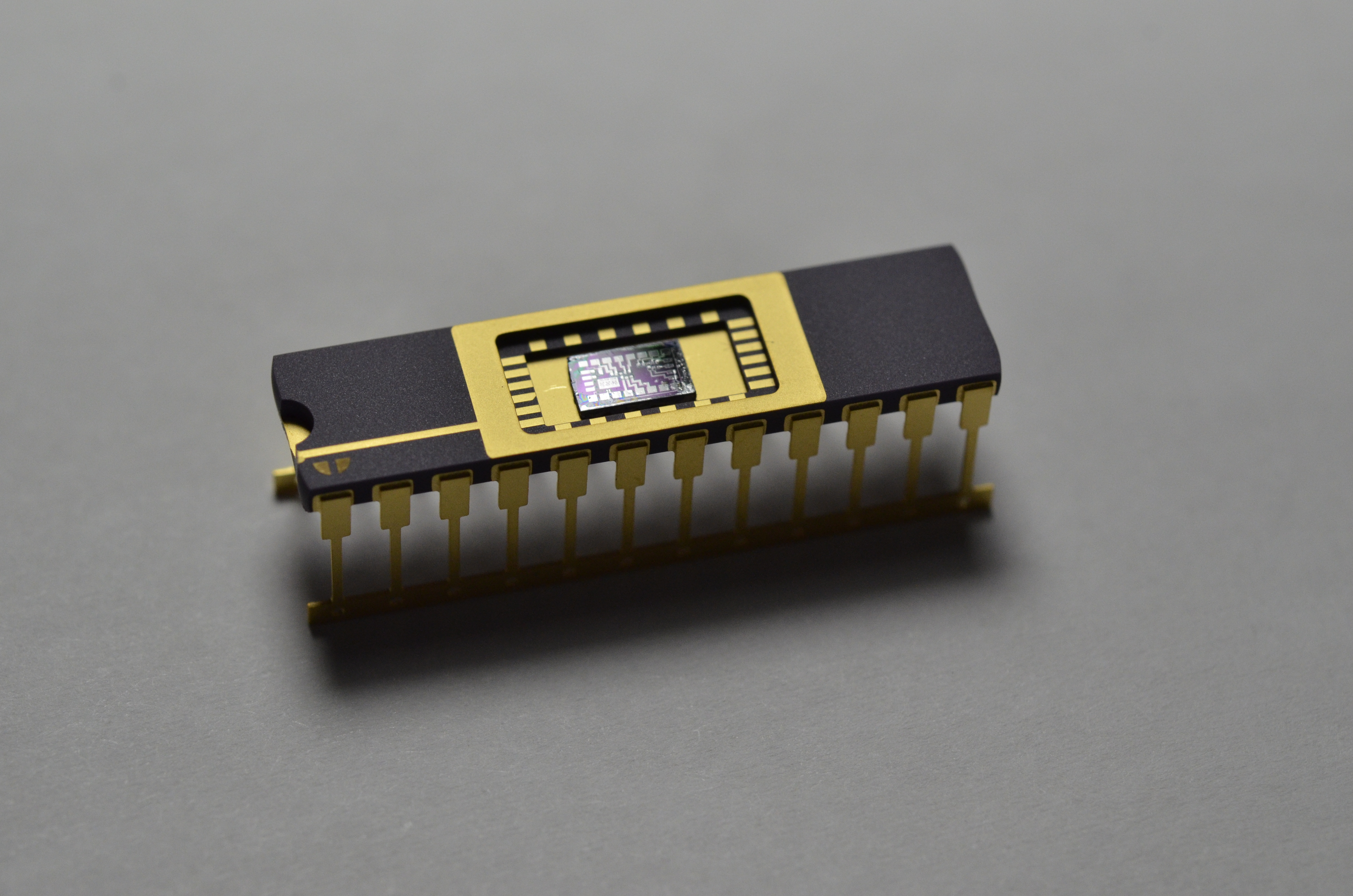
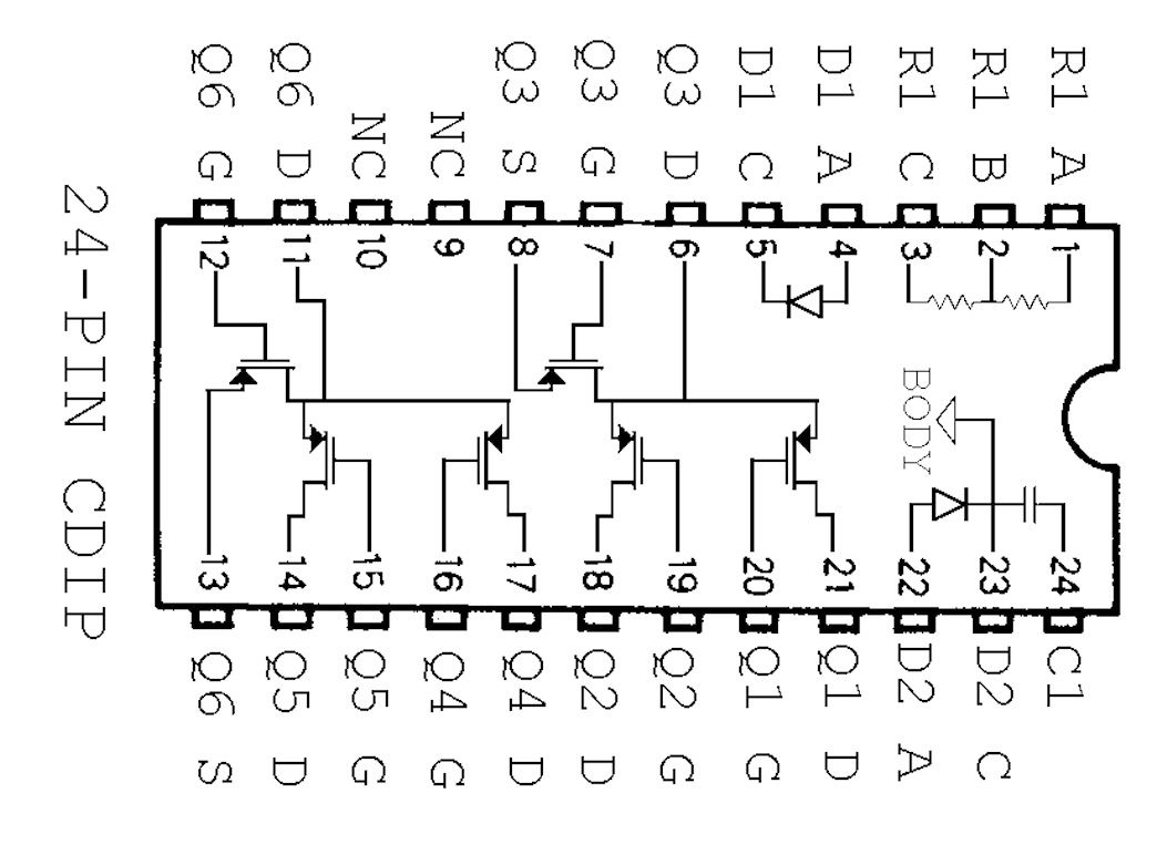
50mm <100> orientation Silicon wafers with bulk resistivity 1 to 10 Ω-cm (30.8 to 308 Ω/sq for thickness of 325µm) are scored into 5.08 x 3.175mm dies (~16mm^2 area) with an Epilog fiber laser. Polyvinyl Alcohol in water or photoresist can be spun on the wafer prior to laser scribing to “catch” laser ablation debris and the film is later removed in solvent before processing. This die size is chosen to fit into a Kyocera 24pin DIP carrier.
Native oxide is stripped off the wafer with a quick dilute HF dip and then they are extensively cleaned in Piranha solution (H2SO4:H2O2), RCA 1 (H2O:NH3:H2O2), RCA 2 (H2O:HCL:H2O2), followed by another dilute HF dip. Most of these cleaning dips are for 10 minutes and can be facilitated by raising to ~40ºC.
The field oxide is thermally grown in a water vapor ambient (wet oxidation) to a thickness of 5000-8000Å. One may consider mixing the DI water for this step with a few percent HCl. The Chrloine atoms help getter and immobilize ionic contaminants and are also said to increase the growth rate by 5-7%. Together with the fact I am making PMOS devices rather than NMOS, these give a huge edge over contamination control and allow decently preforming devices to be fabricated in a garage.
The oxidized wafer is ready for patterning of the active/doped (P-type) area. Positive photoresist (AZ MiR 701 for SiO2 patterning and AZ 4210 for Al layer) is spun on at around 3000rpm yielding a film of about 1.5μm for the AZ MiR 701 or 3.5μm for the AZ 4210 which is soft baked at 90C on a hotplate.
The active area mask is exposed with my Mark IV maskless photolithography stepper at 365nm UV and the pattern is developed in TMAH or KOH solution depending on the resist.

The resist pattern is then hard baked and a number of other tricks are used to ensure good resist adhesion and chemical stability during the following HF etch step which transfers that pattern to the oxide layer and opens windows to the bare silicon surface for doping. These regions later become the source/drain of the FETs.


Doping is then carried out by either solid or liquid source. The solid source is a Boron Nitride disk that is placed in proximity (<2mm) from the wafer in the tube furnace. Alternatively, spin-on liquid sources can be prepared from Phosphoric or Boric acid in water or solvents and doping is carried out in a standard pre-deposition/HF dip/drive-in/deglaze process. I obtained Phosphoric acid in pure form on Amazon and Boric acid from Roach & Ant killer. Since the starting wafer for PMOS here is N-type, I am doing P diffusions of Boron for the source/drain regions and am targeting a sheet resistance in diffused regions of 100 to 250 Ω/sq.
The above mentioned patterning steps are then repeated twice for the gate oxide layer and then the contact layer. The gate oxide must be much thinner (<~750Å) than the field oxide, so the regions between the source/drain are etched away and a thinner oxide is grown there. Then, since the whole wafer has been oxidized during the doping step, contact windows must be etched for the metal layer to make connection with source/drain doped regions.


(click to enlarge)
Now, all the transistors are formed and are ready to be interconnected and broken out to the lead frame. A blanket layer of Aluminum (400-500nm) is sputtered or thermally evaporated onto the wafer. An alternative would be to use the lift-off process in which the photoresist is patterned first and then metal is deposited. To support wire bonding, this metal layer is made thicker (around 2.5µm for Au wire wedge bonding.) These films have a measured bulk resistivity around 5.4e-6 Ω-cm for thermally evaporated films, double the ideal value of 2.7e-6 Ω-cm for Al at 20ºC. The incorporation of Oxygen and other gasses into the Al film during vacuum deposition likely accounts for this difference.

The metal layer is then patterned with photolithography and etched in hot Phosphoric acid (50ºC) to yield the completed IC. The final steps before testing are visual inspection and high temperature annealing of the Aluminum to create ohmic connections.


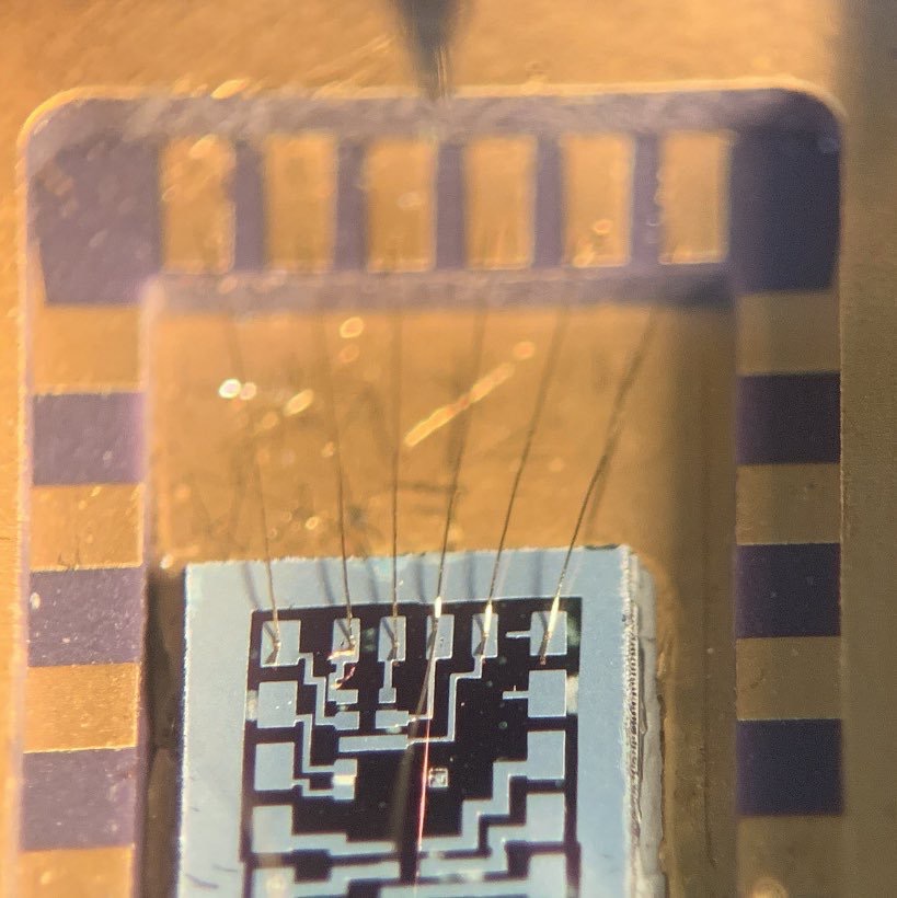
The finished chip is now ready for packaging and testing.
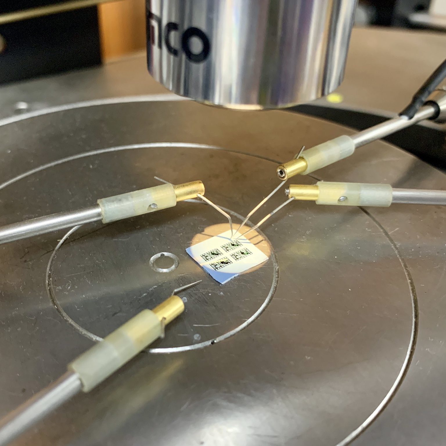
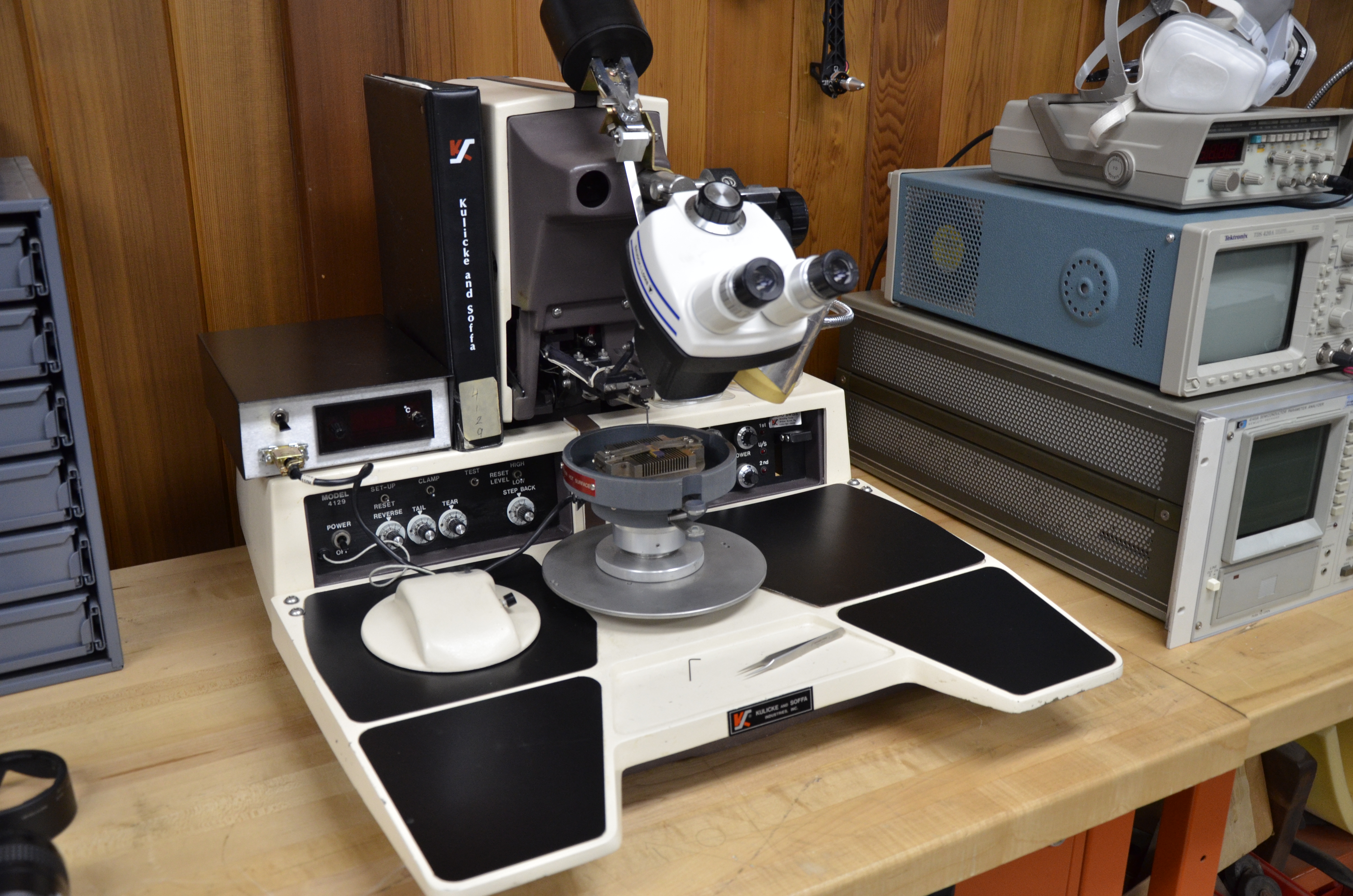
I don’t have a wire bonder (accepting donations!) so my testing right now is limited to manually probing the wafer with sharp tweezers or using a flip-chip board (difficult to align) to connect it to a curve tracer. The differential amplifier is also tested empirically in-circuit to verify operation.
EDIT: see update at the bottom, I now have a wire bonder!


As you can see above in the PMOS FET Id vs. Vds curves, there is lots of die to die variation and devices made on the same day can have widely different characteristics. Taking 5 traces with -1V Vgs increment requires about a -8V body/substrate bias to overcome fixed charges (positive impurity ions trapped under gate) and lattice defects in the gate region and yield the expected graph.
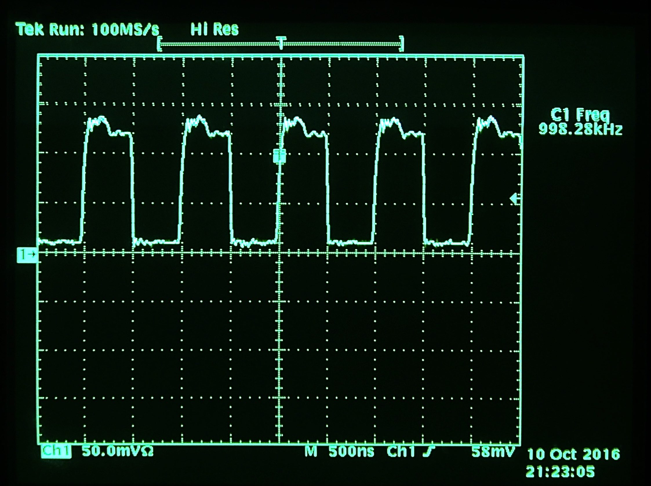
The chip can also be wired as a 3 stage ring oscillator, the classic test for a new IC fabrication process:
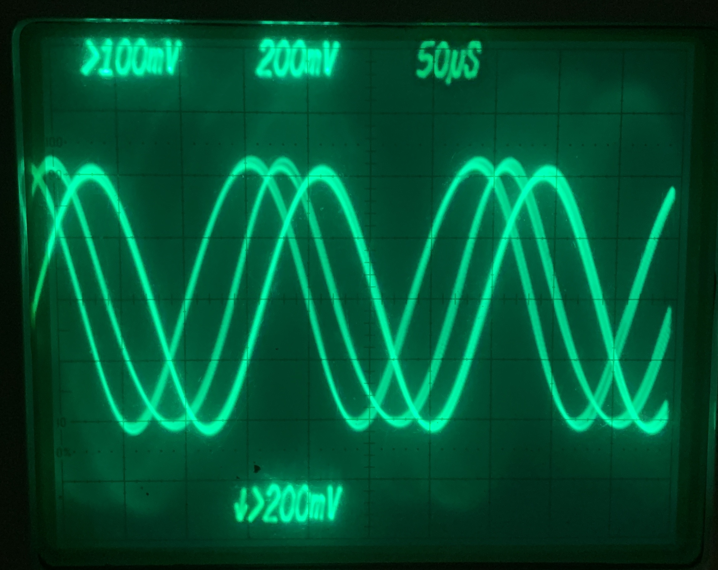

Showing a natural frequency of around 5kHz for 3 stages, limited mainly by excess the gate to source capacitance due to lithography alignment limitations.
Chips can be tested easily and repeatably by probing or wire bonding.
Electrical characteristics of Al/Si junctions are characterized as well and show the expected results. We can create three such basic contacts between Aluminum and Silicon. Aluminum is P-type with respect to Silicon so Schottky diodes are formed whenever Aluminum comes into contact with lightly doped N Silicon. Sometimes my devices showed a tunneling characteristic rather than the expected diode, so I theorize that if the same device is processed for a longer time under high temperatures (>1000ºC), increased oxidation at the Si surface causes the Phosphorous at the surface of the wafer to “pile-up” because of the increased solubility of N-type dopant in SiO2. This creates an “N+” region at the surface and the higher dopant concentration creates a diminishing depletion layer which relates to a small potential energy barrier (the electrons can easily tunnel across it), explaining the symmetrical IV curve.
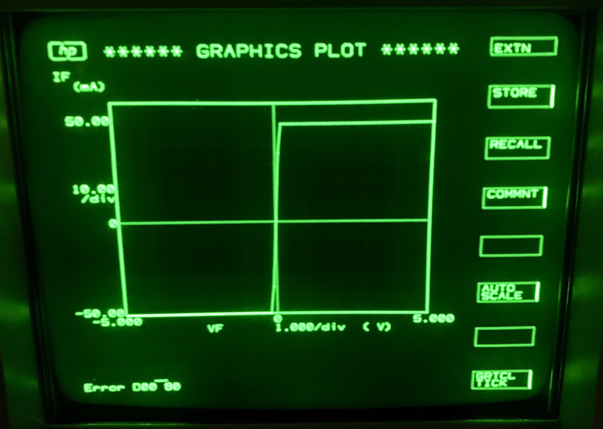


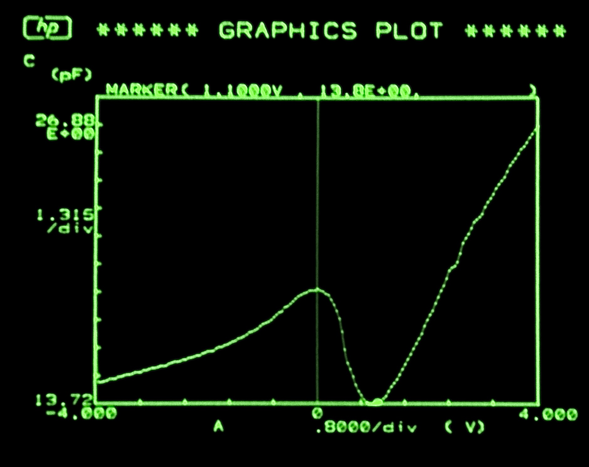
Additionally, the gate oxide dielectric breakdown voltage can be destructively tested. For high quality SiO2, this should be a little over 1V/nm and is easily tested by sweeping Vgs up from 0V and noticing when a large current flows (in normal operation the gate is insulating and no current should be able to flow).

This plot shows gate dielectric breakdown occurring at 21.7V for a 25nm thick gate device, indicating a decent thermally grown oxide quality which could be improved by being grown in an atmosphere with higher Nitrogen content.
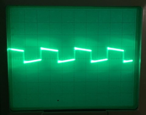
The switching and differential amplifier characteristics can also be demonstrated. The trace on the right shows the output of the chip configured as a fully differential amplifier, mixing (adding/subtracting) a 1kHz and 50kHz sine waves together.


The final characteristic to test for is a low-leakage, fully insulating gate as one of the main requirements of true MOSFET operation. As you can see, I am able to charge up the gate of the device and turn it on through a high impedance connection through my fingertip, and the 1, 0 states of the FET are “latching” due to charge staying on the gate of the FETs and having no pathway to dissipate.
Long ago, some amplifiers were plagued with “popcorn” or burst noise, thought to be caused from random events in defects within the semiconductor. This manifests as large step-impulse changes in the output and has been virtually eliminated in modern ICs due to improved material purity and processing cleanliness. However, some of the devices I made exhibit tons of popcorn noise, shown in the video below (noise in differential pair is amplified on scope, zero input creates hundreds of millivolt output). One of my favorite quotes on this type of noise was said by an engineer in reference to the MAX9776, “You could measure it with a frog’s leg and a stopwatch.” Mine clearly falls in this category…
Update 9/3/18: I got a wire bonder (K&S Al/Au wedge bonder)! It will definitely take some more practice before I can bond to a chip, but results will be posted. This will also allow for more extensive testing. I just moved out to college so progress will hopefully be made on school breaks. A huge thanks to Jeremy Gordon (@JeremySF on Twitter) for the gracious donation.

Update 7/8/19: FET gate length (feature size) reduced to <5µm, bringing this project to be state-of-the-art in about 1975 and allows the transistors to operate with much better characteristics. Pictured below is a ~4.5µm Aluminum gate and the corresponding characteristics showing 5 traces, -3V step and a -8V body/substrate bias.


Thanks for following my work and feel free to contact me with your thoughts!
Details and photos of my newest maskless photolithography stepper have been posted here: Info Page
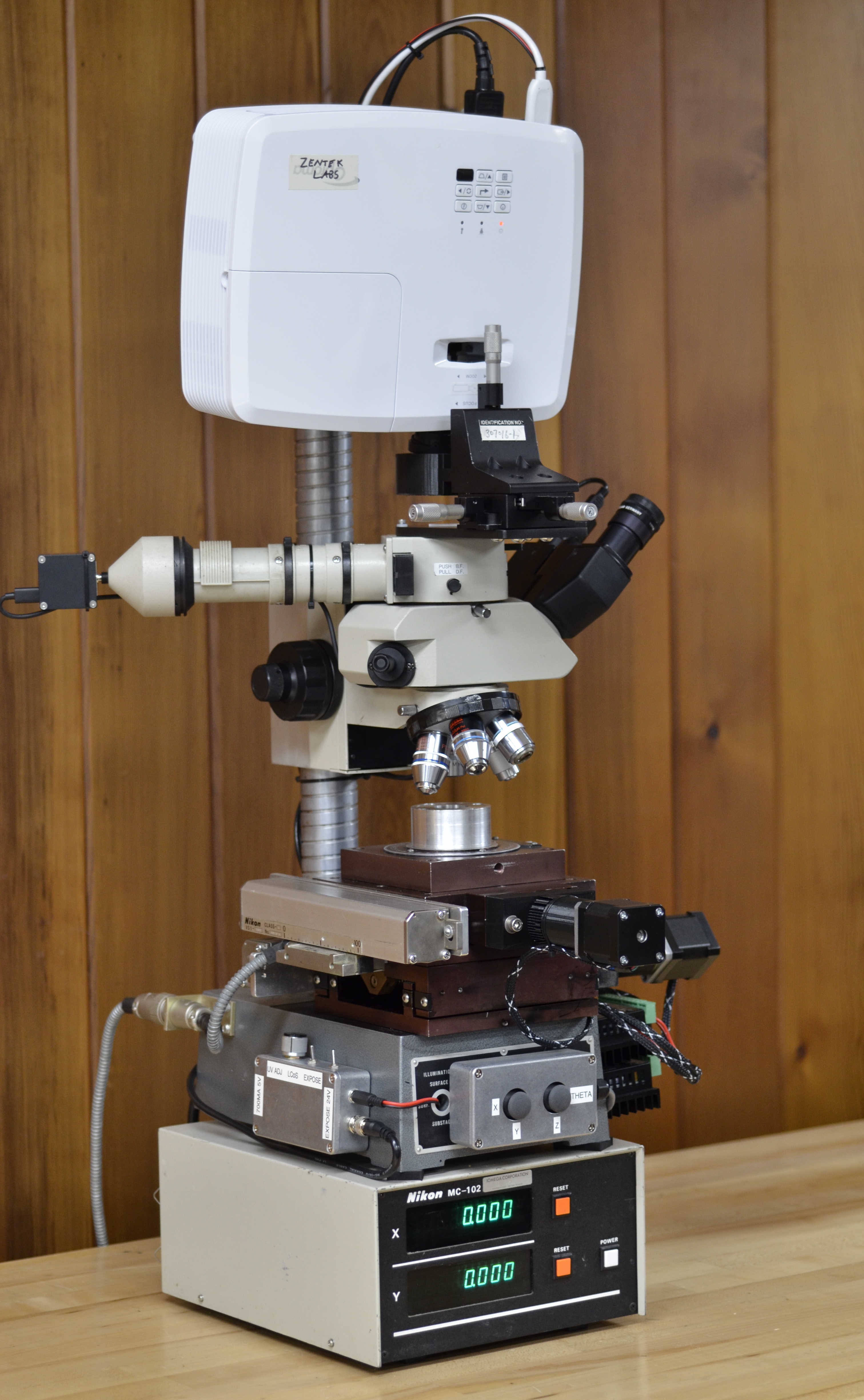
Automated DLP submicron stepper for 2″ (50mm) wafers with LabView control, computer alignment, and wafer vacuum chuck. Based on an old Nikon microscope with custom optics and in-situ UV-VIS spectroscopy for illumination process control. Diffraction-limited resolution is <250nm with a 365nm light source.
