Update 4/25/18: First IC!
Update 8/27/17: Developing Patterning Process for Homemade Microelectronics
Update 7/30/17: Developing Metalization Process for Homemade Microelectronics
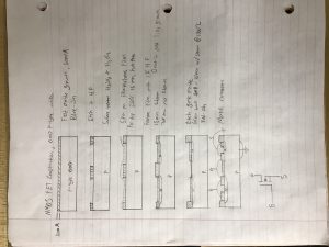

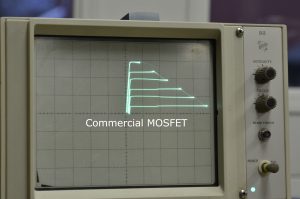
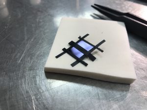


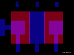
These are my first working transistors. Specifically, they are insulated gate enhancement mode n channel field effect transistors. I also made a depletion mode FET with a conducting channel and it worked even better than the enhancement mode ones. I drew out the steps I took to make this, they’re based on Jeri Ellsworth’s work but with a few main changes. It is very important that your dielectric overlap source and drain regions on the FET, otherwise no inversion layer can be formed and the FET cannot turn on. Only a small overlap is necessary and the larger it is, the more unwanted capacitance there is. This is not normally a consideration in actual production because inherent lateral diffusion takes care of the overlap but for these large hand made devices I found you have to get very lucky with your alignment if you don’t budget extra overlap.
A huge thanks to Jeri for making her videos about home chip fabrication which got me interested in these experiments in the first place.
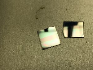
You can see in the center of the transistor there is a red region of silicon dioxide, this is the gate and the color indicates that it is roughly 750 angstroms thick. I would like to make the gate thinner so I can achieve lower threshold voltages, etc. but it is hard to make a truly insulating gate much thinner than that in a dirty environment because of pinholes and other impurities in the oxide layer.


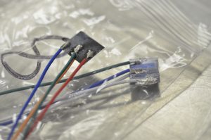
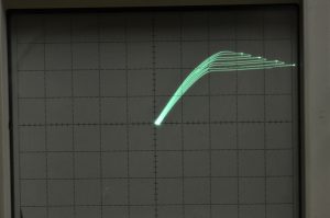
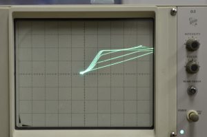
Diode characteristics are characterized with a semiconductor parameter analyzer
A brief introduction to semiconductor fabrication processes and terminology. It is not intended to be an in depth view of any single process, but rather an overview so that provides enough information for someone to get started with making diodes and transistors at home.
Tour of my home chip fab setup in early 2017. I’ve been accumulating this equipment since October of 2016.
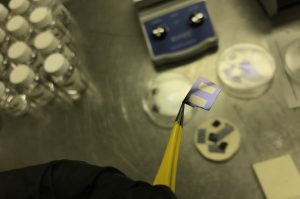
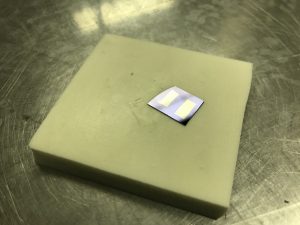
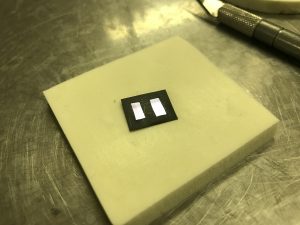
Step by step FET fabrication
Wow wonder if it’s possible to do bipolar?