Homemade computer chips / integrated circuits
Preface
I am very excited to announce details of the first homemade integrated circuit and share the journey that this project has taken me on over the past year. I hope that my success will inspire others and help start a revolution in home chip fabrication. When I set out on this project I had no idea of what I had gotten myself into, but in the end I learned more than I ever thought I would about physics, chemistry, optics, electronics, and so many other fields. Furthermore, my efforts have only been matched with the most positive feedback and support from the world; I owe a sincere thanks to everyone who has helped me, given me advice, and inspired me on this project. Especially my amazing parents, who not only support and encourage me in any way they can but also give me a space to work in and put up with the electricity costs… Thank you!
Let’s democratize the tools of innovation.
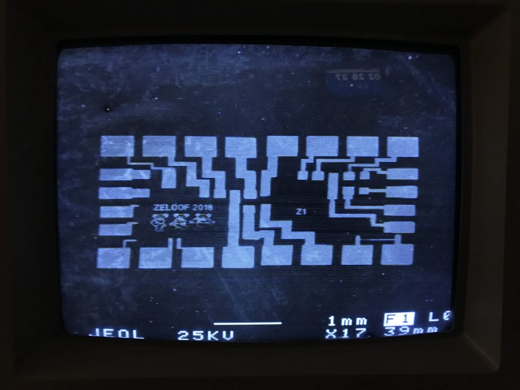
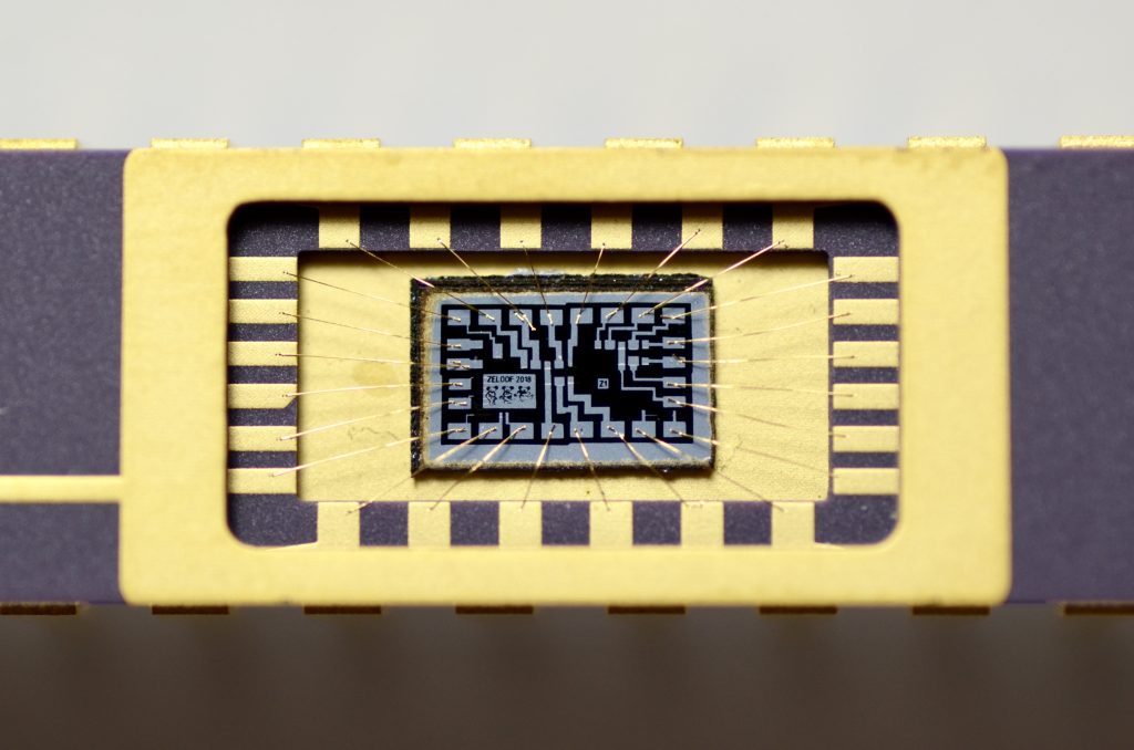
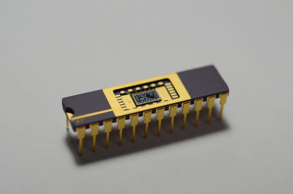 I present the first homemade (lithographically-fabricated) integrated circuit – the “Z1” PMOS dual differential amplifier chip. I say “lithographically-fabricated” because Jeri Ellsworth made the first transistors and logic gates (meticulously hand wired with conductive epoxy) and showed the world that this is possible. Inspired by her work, I have demonstrated ICs made by a scalable, industry-standard, photolithographic process. Needless to say, this is the logical step-up from my previous replication of Jeri’s FET fabrication work.
Design
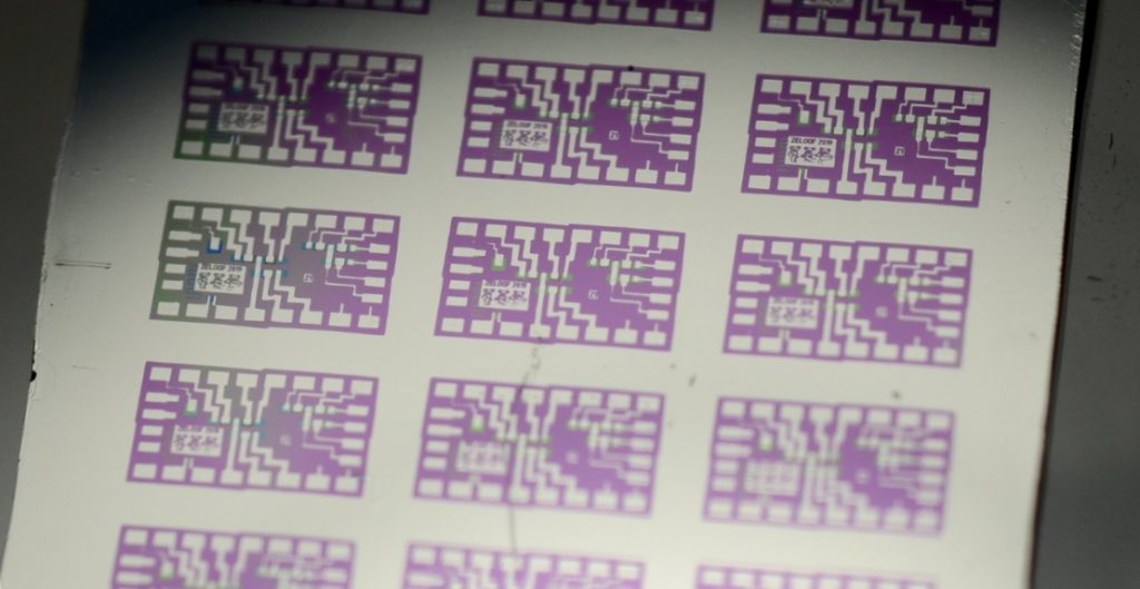
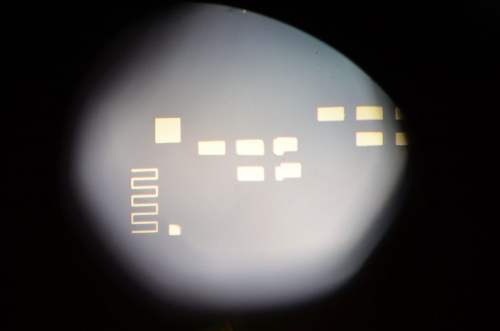
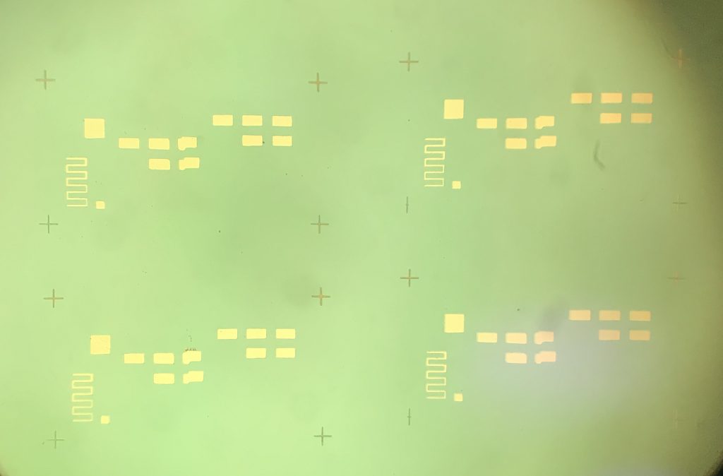
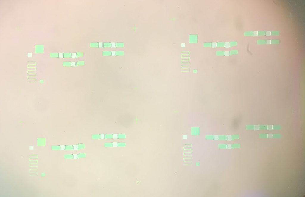
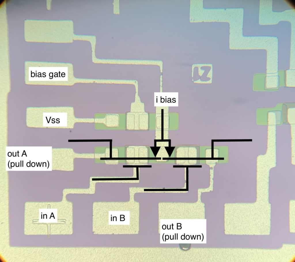
I designed the Z1 amplifier looking for a simple chip to test and tweak my process. Layout was done in Magic VLSI for a 4 mask PMOS process (active/doped area, gate oxide, contact window, and top metal.) PMOS has advantages over NMOS as far as mobile ionic contamination that lends it to being fabricated in a garage. The masks are designed in 16:9 aspect ratio for easy projection.
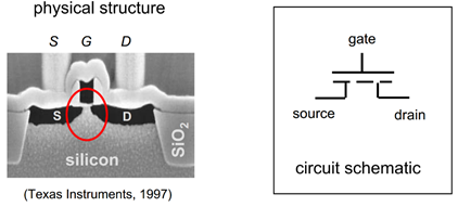
The feature (gate) size is approximately 175μm although there are test features as small as 2μm on the chip. Each amplifier section (center and right) contain 3 transistors (2 for long-tailed differential pair and one as current source/load resistor) which means a total of 6 FETs on the IC. The left portion of the IC contains resistors, capacitors, diodes, and other test features used to characterize the fabrication process. Each node of the differential pairs is broken out to a separate pin on the lead frame so it can be analyzed and external biasing can be added as necessary.
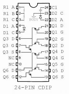
EDIT: see update at the bottom, the transistor gate length has been reduced to <5µm (1975 tech. level) which brings an increase in device performance.
Fabrication
There are 66 individual fabrication steps to make this chip and it takes approximately 12 hours for a full run. The process yield can be as high as 80% for these large features, but is largely dependent on my coffee intake that day. I have also made Youtube videos covering semiconductor fabrication theory and discrete MOSFET fabrication.
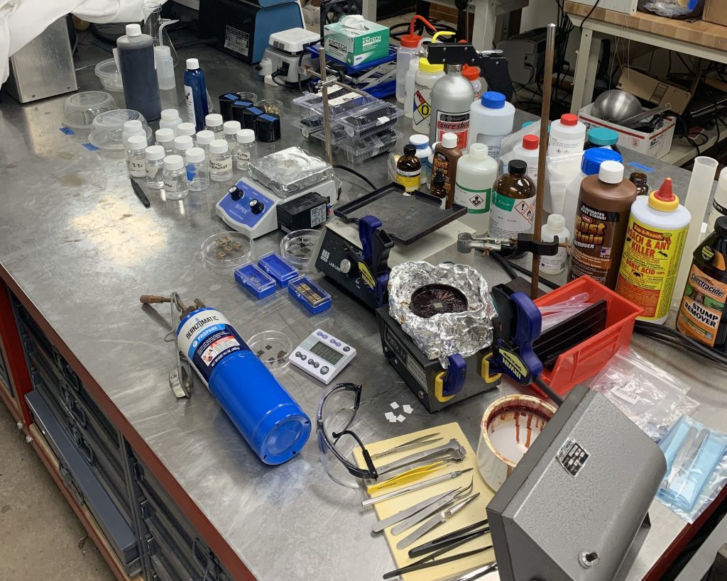
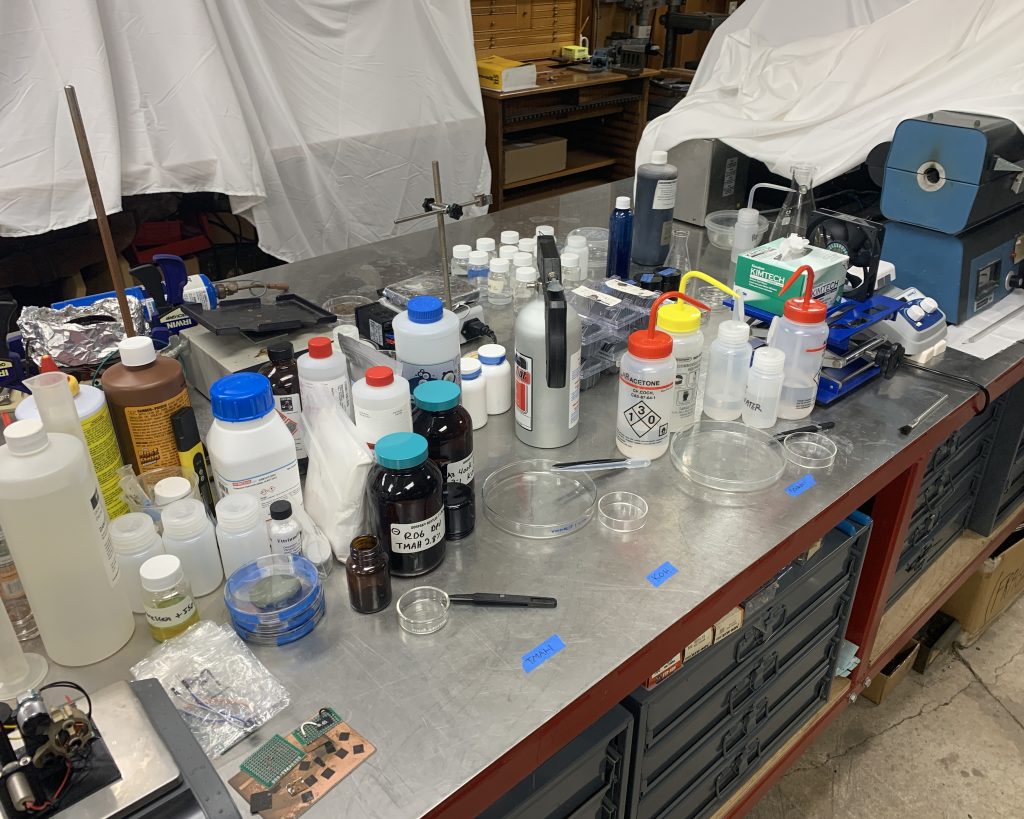
The home chip fab chemistry bench is pictured below and basically includes everything needed to manufacture ICs except a vacuum chamber and a lithography setup. More information about equipment and chemicals is in my Supercon talk from 2018.
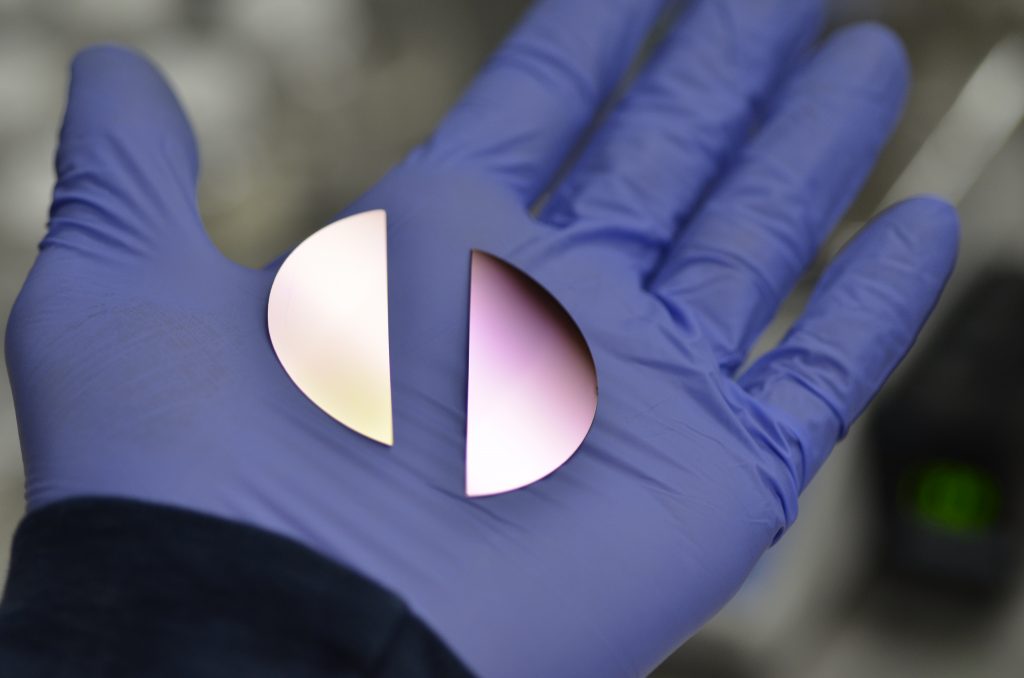
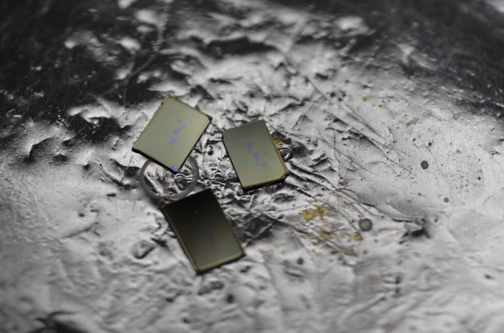
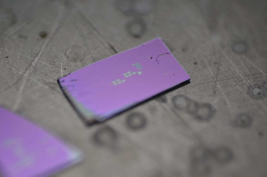
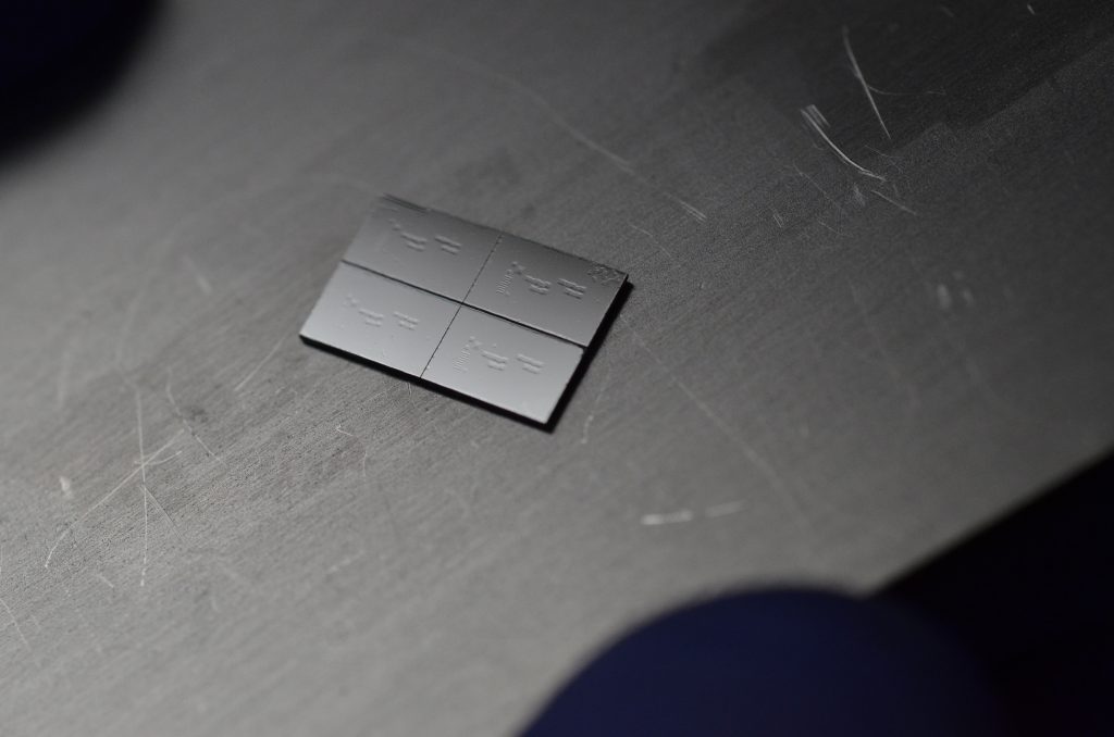
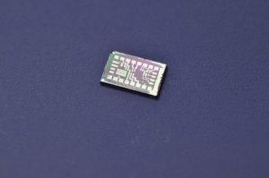
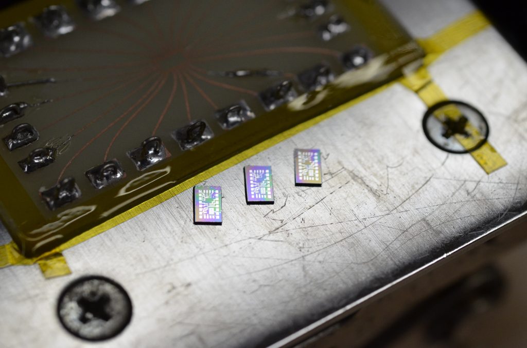
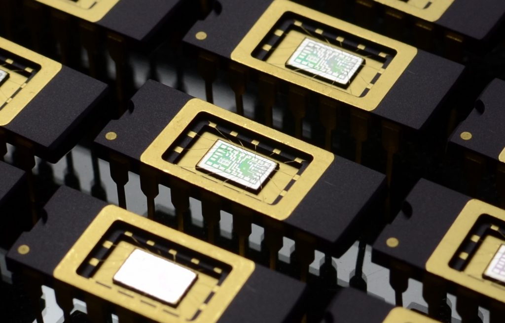
50mm <100> orientation Silicon wafers with bulk resistivity 1 to 10 Ω-cm (30.8 to 308 Ω/sq for thickness of 325µm) are scored into 5.08 x 3.175mm dies (~16mm^2 area) with an Epilog fiber laser. Polyvinyl Alcohol in water or photoresist can be spun on the wafer prior to laser scribing to “catch” laser ablation debris and the film is later removed in solvent before processing. This die size is chosen to fit into a Kyocera 24pin DIP carrier.
Native oxide is stripped off the wafer with a quick dilute HF dip and then they are extensively cleaned in Piranha solution (H2SO4:H2O2), RCA 1 (H2O:NH3:H2O2), RCA 2 (H2O:HCL:H2O2), followed by another dilute HF dip. Most of these cleaning dips are for 10 minutes and can be facilitated by raising to ~40ºC.
The field oxide is thermally grown in a water vapor ambient (wet oxidation) to a thickness of 5000-8000Å. One may consider mixing the DI water for this step with a few percent HCl. The Chrloine atoms help getter and immobilize ionic contaminants and are also said to increase the growth rate by 5-7%. Together with the fact I am making PMOS devices rather than NMOS, these give a huge edge over contamination control and allow decently preforming devices to be fabricated in a garage.
The oxidized wafer is ready for patterning of the active/doped (P-type) area. Positive photoresist (AZ MiR 701 for SiO2 patterning and AZ 4210 for Al layer) is spun on at around 3000rpm yielding a film of about 1.5μm for the AZ MiR 701 or 3.5μm for the AZ 4210 which is soft baked at 90C on a hotplate.
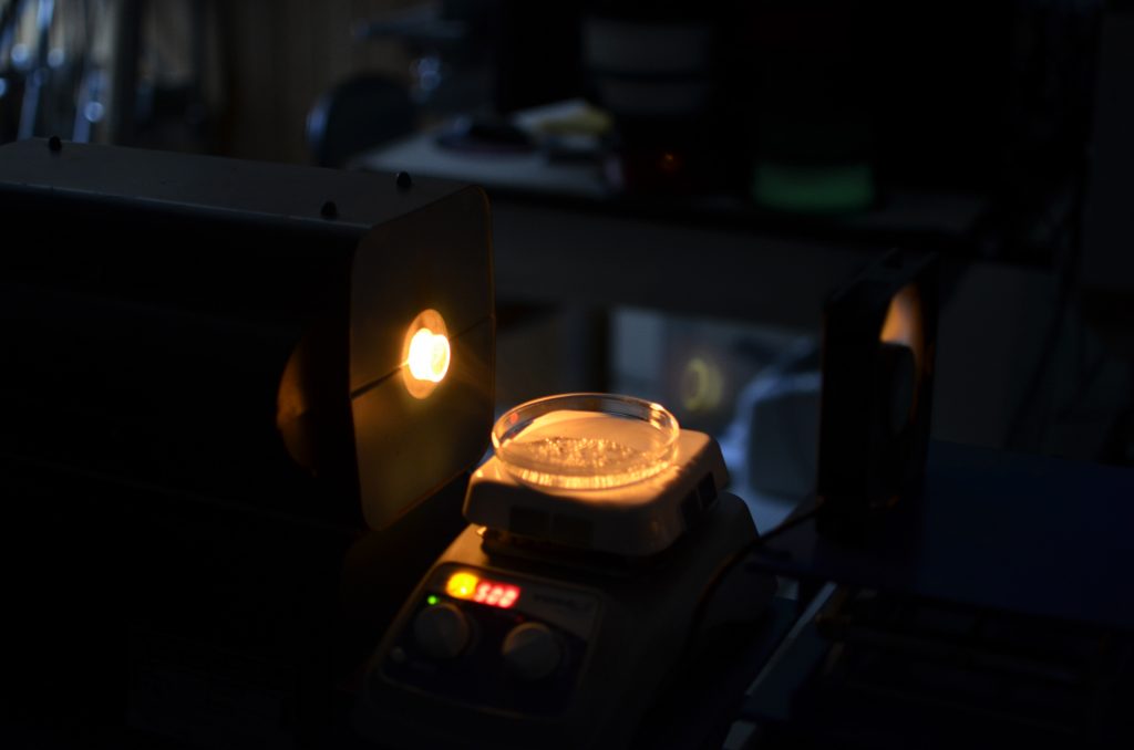
The active area mask is exposed with my Mark IV maskless photolithography stepper at 365nm UV and the pattern is developed in TMAH or KOH solution depending on the resist.
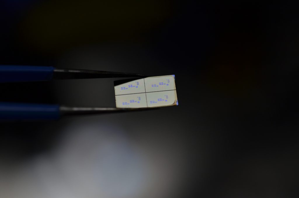
The resist pattern is then hard baked and a number of other tricks are used to ensure good resist adhesion and chemical stability during the following HF etch step which transfers that pattern to the oxide layer and opens windows to the bare silicon surface for doping. These regions later become the source/drain of the FETs.
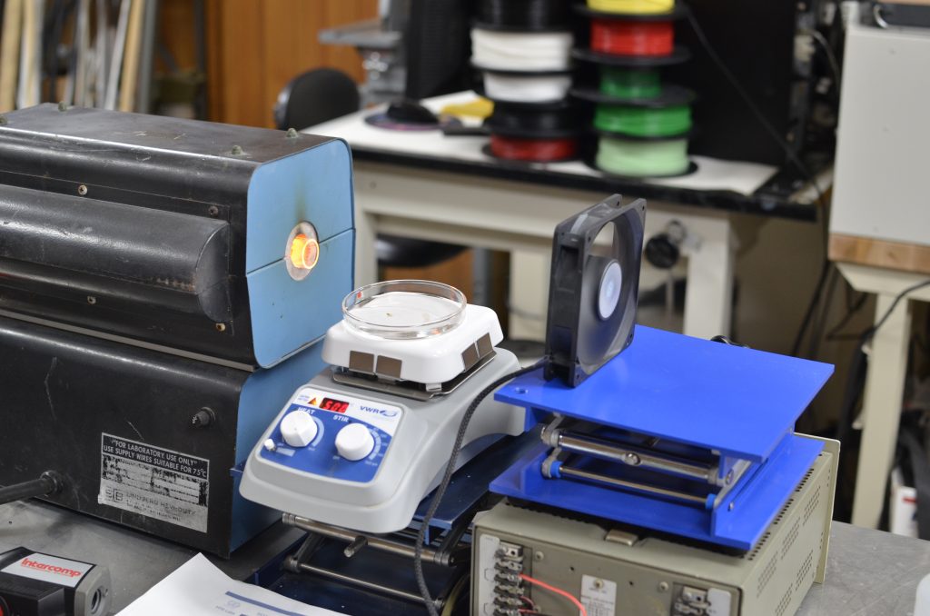
Doping is then carried out by either solid or liquid source. The solid source is a Boron Nitride disk that is placed in proximity (<2mm) from the wafer in the tube furnace. Alternatively, spin-on liquid sources can be prepared from Phosphoric or Boric acid in water or solvents and doping is carried out in a standard pre-deposition/HF dip/drive-in/deglaze process. I obtained Phosphoric acid in pure form on Amazon and Boric acid from Roach & Ant killer. Since the starting wafer for PMOS here is N-type, I am doing P diffusions of Boron for the source/drain regions and am targeting a sheet resistance in diffused regions of 100 to 250 Ω/sq.
The above mentioned patterning steps are then repeated twice for the gate oxide layer and then the contact layer. The gate oxide must be much thinner (<~750Å) than the field oxide, so the regions between the source/drain are etched away and a thinner oxide is grown there. Then, since the whole wafer has been oxidized during the doping step, contact windows must be etched for the metal layer to make connection with source/drain doped regions.
(click to enlarge)
Now, all the transistors are formed and are ready to be interconnected and broken out to the lead frame. A blanket layer of Aluminum (400-500nm) is sputtered or thermally evaporated onto the wafer. An alternative would be to use the lift-off process in which the photoresist is patterned first and then metal is deposited. To support wire bonding, this metal layer is made thicker (around 2.5µm for Au wire wedge bonding.) These films have a measured bulk resistivity around 5.4e-6 Ω-cm for thermally evaporated films, double the ideal value of 2.7e-6 Ω-cm for Al at 20ºC. The incorporation of Oxygen and other gasses into the Al film during vacuum deposition likely accounts for this difference.
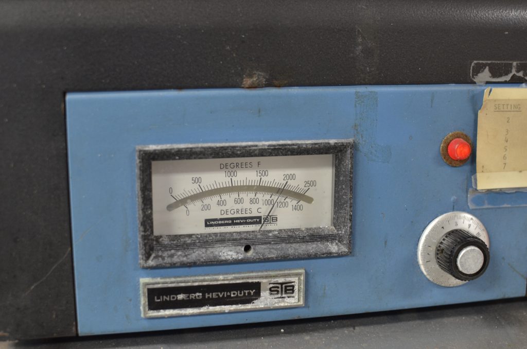
The metal layer is then patterned with photolithography and etched in hot Phosphoric acid (50ºC) to yield the completed IC. The final steps before testing are visual inspection and high temperature annealing of the Aluminum to create ohmic connections.
The finished chip is now ready for packaging and testing.
Testing
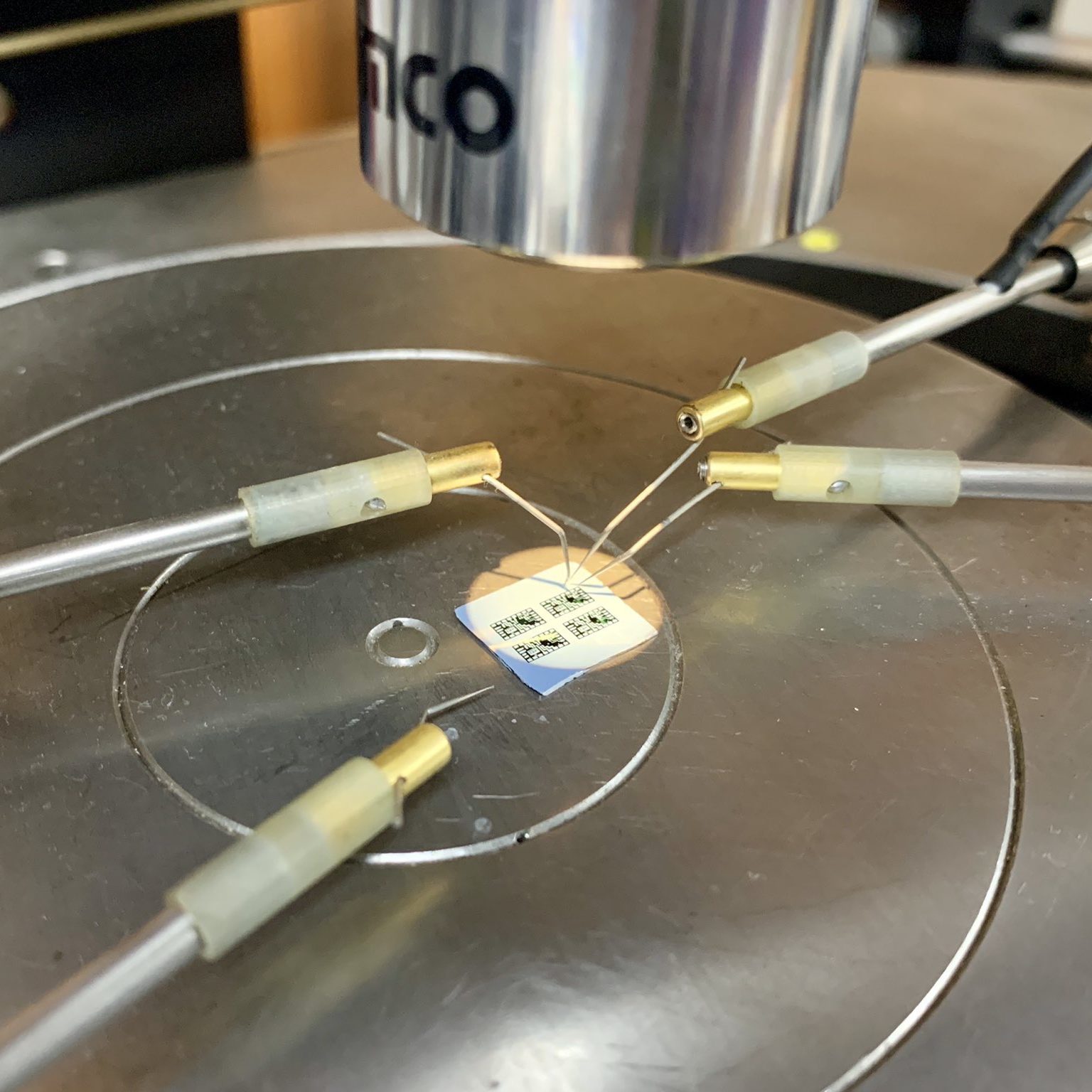
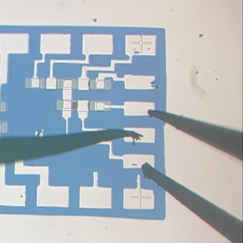
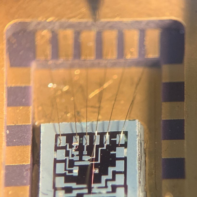
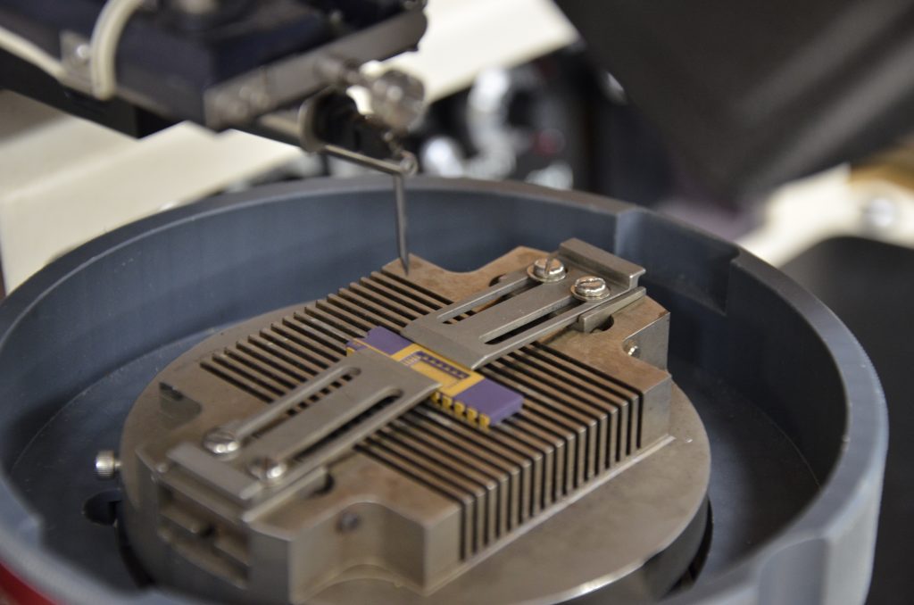
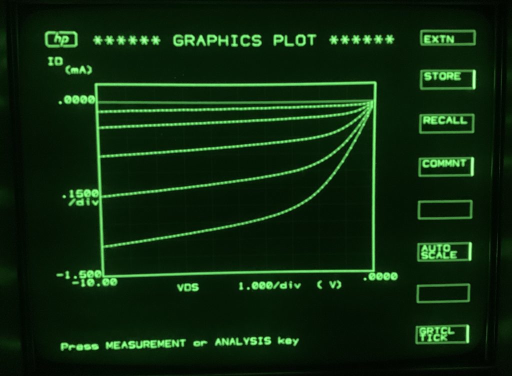
I don’t have a wire bonder (accepting donations!) so my testing right now is limited to manually probing the wafer with sharp tweezers or using a flip-chip board (difficult to align) to connect it to a curve tracer. The differential amplifier is also tested empirically in-circuit to verify operation.
EDIT: see update at the bottom, I now have a wire bonder!
As you can see above in the PMOS FET Id vs. Vds curves, there is lots of die to die variation and devices made on the same day can have widely different characteristics. Taking 5 traces with -1V Vgs increment requires about a -8V body/substrate bias to overcome fixed charges (positive impurity ions trapped under gate) and lattice defects in the gate region and yield the expected graph.
The chip can also be wired as a 3 stage ring oscillator, the classic test for a new IC fabrication process:
Showing a natural frequency of around 5kHz for 3 stages, limited mainly by excess the gate to source capacitance due to lithography alignment limitations.
Chips can be tested easily and repeatably by probing or wire bonding.
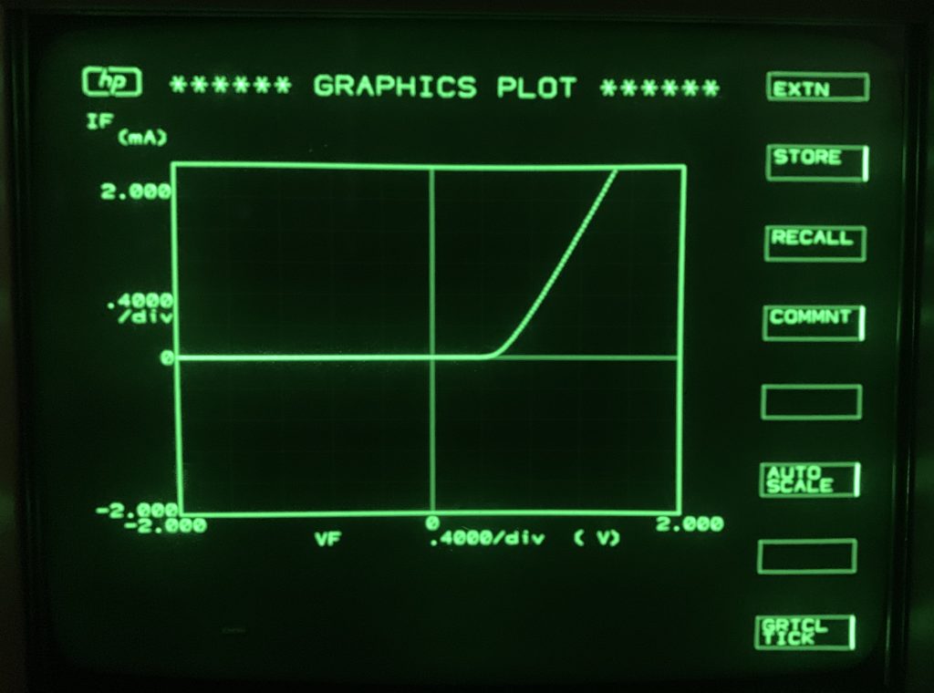
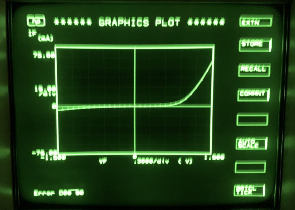
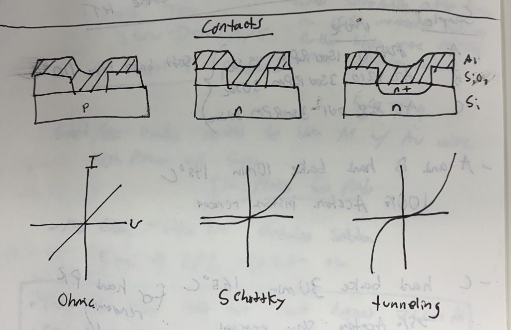
Electrical characteristics of Al/Si junctions are characterized as well and show the expected results. We can create three such basic contacts between Aluminum and Silicon. Aluminum is P-type with respect to Silicon so Schottky diodes are formed whenever Aluminum comes into contact with lightly doped N Silicon. Sometimes my devices showed a tunneling characteristic rather than the expected diode, so I theorize that if the same device is processed for a longer time under high temperatures (>1000ºC), increased oxidation at the Si surface causes the Phosphorous at the surface of the wafer to “pile-up” because of the increased solubility of N-type dopant in SiO2. This creates an “N+” region at the surface and the higher dopant concentration creates a diminishing depletion layer which relates to a small potential energy barrier (the electrons can easily tunnel across it), explaining the symmetrical IV curve.
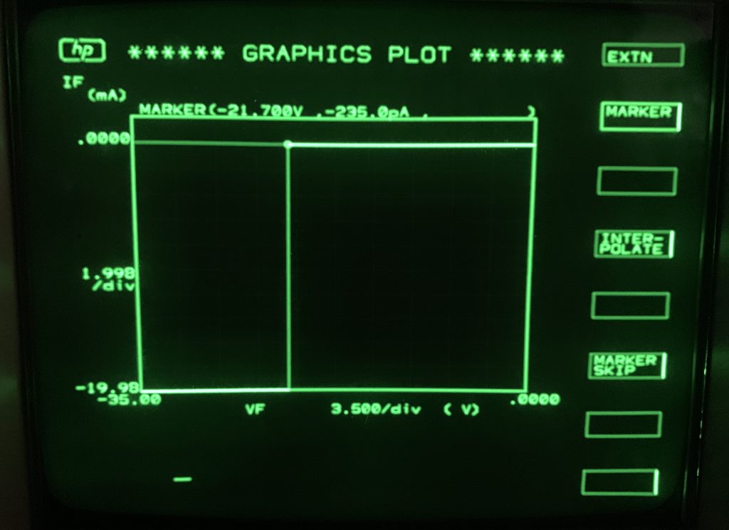
Additionally, the gate oxide dielectric breakdown voltage can be destructively tested. For high quality SiO2, this should be a little over 1V/nm and is easily tested by sweeping Vgs up from 0V and noticing when a large current flows (in normal operation the gate is insulating and no current should be able to flow).
This plot shows gate dielectric breakdown occurring at 21.7V for a 25nm thick gate device, indicating a decent thermally grown oxide quality which could be improved by being grown in an atmosphere with higher Nitrogen content.
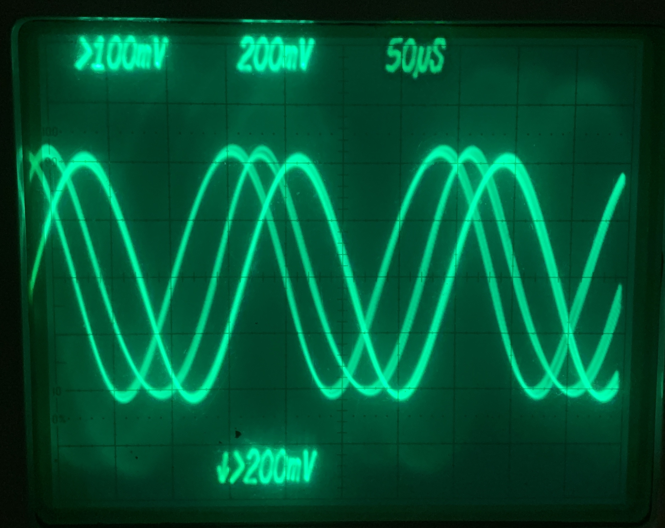
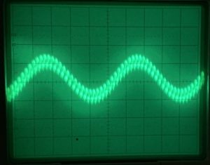
The switching and differential amplifier characteristics can also be demonstrated. The trace on the right shows the output of the chip configured as a fully differential amplifier, mixing (adding/subtracting) a 1kHz and 50kHz sine waves together.
The final characteristic to test for is a low-leakage, fully insulating gate as one of the main requirements of true MOSFET operation. As you can see, I am able to charge up the gate of the device and turn it on through a high impedance connection through my fingertip, and the 1, 0 states of the FET are “latching” due to charge staying on the gate of the FETs and having no pathway to dissipate.
Long ago, some amplifiers were plagued with “popcorn” or burst noise, thought to be caused from random events in defects within the semiconductor. This manifests as large step-impulse changes in the output and has been virtually eliminated in modern ICs due to improved material purity and processing cleanliness. However, some of the devices I made exhibit tons of popcorn noise, shown in the video below (noise in differential pair is amplified on scope, zero input creates hundreds of millivolt output). One of my favorite quotes on this type of noise was said by an engineer in reference to the MAX9776, “You could measure it with a frog’s leg and a stopwatch.” Mine clearly falls in this category…
Update 9/3/18: I got a wire bonder (K&S Al/Au wedge bonder)! It will definitely take some more practice before I can bond to a chip, but results will be posted. This will also allow for more extensive testing. I just moved out to college so progress will hopefully be made on school breaks. A huge thanks to Jeremy Gordon (@JeremySF on Twitter) for the gracious donation.
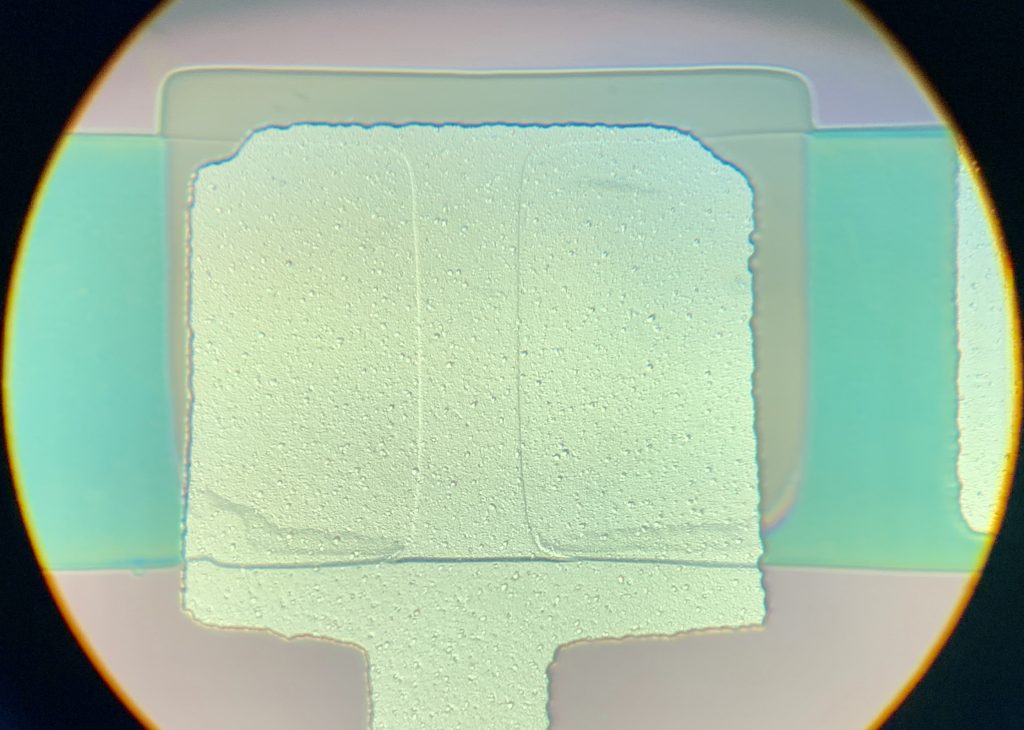
Update 7/8/19: FET gate length (feature size) reduced to <5µm, bringing this project to be state-of-the-art in about 1975 and allows the transistors to operate with much better characteristics. Pictured below is a ~4.5µm Aluminum gate and the corresponding characteristics showing 5 traces, -3V step and a -8V body/substrate bias.
Thanks for following my work and feel free to contact me with your thoughts!
















Thanks for doing such amazing work, this is quite a milestone for everyone in the maker community.
Fantastic project. This can change the IC industry by moving some development to Home IC Fab. Congratulations. Well done.
Hey can you do a video on the complete list of equipment you used?
I hope you make more types of chips.
(Maybe make a motion sensor chip or a chip with some movable part??) That would be something!
No one has done it before.
Regards
Bob Li
We absolutely will do this in our shop next week
Wowsers. My final year uni project was making solar cells so I can appreciate all the fab steps you had to do to make devices, and to do it all by yourself and outside a “lab-enviroment” is just wow/10 man.
How did you manage to get all the equient to do this?
This is amazing, and you should really put your steps together in a book!
How much would it cost me to set up an awesome Fab like yours?
Fascinating! It would be ultra-awesome that this project could be merged with this other: https://dberard.com/home-built-stm/, where he achieves an atom-level resolution scanning electron microscope where a tungsten needle driven by a piezo-actuator scans surfaces and gets a read-out via tunnel effect. You should be neighbour of his garage. 🙂
This is absolutely incredible work. Thank you for taking the extra time of documenting every step as you go and then sharing it with the world.
Your rule! 🙂
I have made a typo.. “you rule!”
This is incredible! DIY IC fabrication is something I had always dreamed about, but the dangers of any kind of vapor deposition process kept me away (as well as the cost of anything approaching proper safety equipment). Well, let’s be honest, the equipment in general is cost-prohibitive unless you want to rely on decommissioned surplus (which is still expensive).
Do you have any comment on the PPE and/or environmental protection considerations you may have (or may not have) undertaken for this project? If that is covered elsewhere in your blog, I apologize for looking over it…
Looks like he’s doing all wet chemistry and vapor/sputter metals (no CVD) so the worst he’s got to deal with is HF and piranha solution but that’s nothing beyond high-school chem lab levels of dangerous.
If he moves on to trying self-aligned gates then the safety/PPE gets to be tricky due to CVD polysilicon which takes silane or trichlorosilane which are super toxic and pyrophoric and all that fun.
Do you have a Patreon account? I cannot support you in any other meaningful way, but I would be very happy if you continued your work. I want to see some decent open CPUs in ~20 years.
Sam,
Simply awesome!
Congratulations on this very important milestone! This is a worthy project indeed.
If you do more complicated circuits, you might consider using closed MOS transistors. In this case it would have saved you one mask (you don’t need “active”) and a few process steps. The university I studied at used the NMOS version of it and you can see the CMOS version created at RCA: http://www.visual6502.org/wiki/index.php?title=RCA_1802E#Simple_logic_gates
Some additional advantages are that you get very nice length/width transistor ratios in a roughly square area and transistors in series get the right sizes for best speed since outer rectangles must be larger than inner ones.
The main problems are that even minimal transistors are a bit large and that all circuits end up connecting to ground (though you can get around that by adding an extra transistor that is always off).
Whoa! Amazing knowledge, patience and whatnot!
This is really spectacular work, Sam! I’m looking forward to your progress and improvements!
This is a fantastic breakthrough Sam,
You are an inspiration to the DIY hardware community.
Super impressive! Now we have hope!
Where is your donate button?
Great work man! You’ll certainly go places with a bar set this high!
Awesome project, the Amp Hour episode was great, too.
Are you aware of this project: https://code.google.com/archive/p/homecmos/ ? It isn’t active anymore, but maybe you can find some useful stuff in the archive.
Would you mind sharing your Magic VLSI design files on GitHub or something for others to play around with? That would be great!
We are still living in 2018, while you are already living in 3018.
Love the logo you used! Keep the Dead alive!
Congratulation ! I can’t tell more. It’s just…
I would like to know every steps in detail and documentation on how you did it.
Just in case one day I have a time, money and a garage at the same time…
Awesome project! Are you going to make microprocessors next?
Your an inspiration. Keep up the good work
Hey, I was “dreaming” just about this a few months ago and thought: “how great would that be!”! (to make that technology commonly available etc… in a e.g. makerspace)
Today, out of curiousity i googled “DIY Integrated Circuit” and your site popped up.
What a New-Year-Gift; keep up the great work – you got my blessing, if that means anything,
best whishes,
Chris
Hi,
Have you seen LibreSilicon project?
Do you think you could use this process in your “fab”?
Cheers and good luck 😉
You’re crowdfunding a replacement for the LTC 6419?
https://www.analog.com/media/en/technical-documentation/data-sheets/6419fa.pdf
My name is mohd faizan
I have compeleted b.tech with electronics and communication.
Actually i am interested to design computer chip. what should i do now?
This is SO inspiring Sam.
I wanted to do something very similar in 1977… construct a transistor for my final year project at college… but was put off the idea by my lecturers because they thought it ‘too complex’. You’re a great inspiration because it just shows that with determination & research, the impossible IS possible.
Just love the write-up and videos. Keep up the great work and I wish you every success in your future endeavours. 🙂
Paul Towle.
Lead Engineer – Electronics
Penso Consulting. UK.
Very inspiring , i wish you all the good luck in your work
Hlw sr I m Pakistan im not english lagvich please my ic NEC 78f0546 not warking please contect mi my whatsapp number 03485573387
Brave job you did there unlike my İ.C. who gave me a degraded mark when İ presented him with 6 seperate digrams of the İ.C. layers; he simply wanted one superimposed large layer of the İ.C.
Sorry; İ.C. doctor
I need to ask how much did it cost,,,,………….?
you are my mith
Thank you so much for your contributions. You are a brillant electrical engineer and fab. cheers!
Hi it’s fantastic ! Aren’t you thinking of selling some of your chips? I would be interested. Congratulations on your success ? Beautiful work ❤️
Amazing work! Congratulations and thank you for sharing!
Impresive work with semiconductos Sam. Been looking around for anyone that can produce a transistor capable of handling 35,000V and 2.5W. This for my own experiment on creating current out of voltage. Which is no more than switching ON and OFF 21 transistors placed in sequence to turn ON and OFF 21 electrodes. What to know if a transistor with these specs is possible? If so can you build it?
Correction: Want to know ,,,?
Sam is it realistic to think in terms of automating this system so that this system consistently produces the product on it’s own, or is that too far in the future? My company is interested in partnering with someone to fashion an advanced model which will equip each of our homes with a system that only requires basic maintenance and resupply. Your work and feedback is appreciated. – Dennis Porter
Very cool 🙂
Hi Sam. I am developing a project seeking to develop very basic electronics off Earth (e.g. Moon) using only local resources. Would you care to participate in Zoom telecon re: this topic? Contact me via: DevelopSpace.info
DevelopSpace.info/electronics
Hi, This is an amazing work at ur garage. This is a great effort u put into. Thanks you for u help.
now I know whom I befriend during a zombie apocalypse! 😀
You are really amazing
So Nice are you human love this inovation.ajmalokara789@gmail.com. plz must be reply I am waiting you Mail till the end of my life.ok
I wanted to do same thing but disappointed ever time why I am so poor no plate farm no money no food every where is darkness.if any body helping our poor flood people Pakistani rupees is so week.if everyone give me a one dollar our day by day Rich plz think so plz.ajmalokara789@gmail.com
I love human love people Pakistani is so so cheating but everyone is no equipment one dollar our life is changing
Congratulations sir, absolutely amazing!