Skip to content
Sam Zeloof

Sam Zeloof

Pages:

  • Contact / About
  • Twitter
  • Looking for the smarter Zeloof Brother?

Categories

  • Electron Microscope
  • Electronics Projects
  • General High Vacuum
  • Home Chip Lab
  • Machining
  • Plasma/Ion Source
  • Uncategorized

Asides

DIY PN Junction Diode Fabrication

thermal oxide growth _500nm closeup thermal oxide growth _500nm 
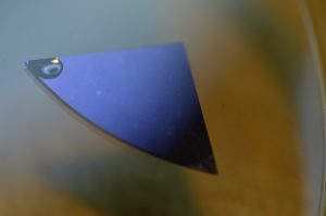
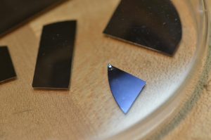
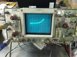
First pictures show wafers with 5000A field oxide, then etched active region for the anode with HF. As you can see on the curve tracer, reverse bias conditions are surprisingly good with little leakage current down to -6 volts.etched active area for dopingimpurities on oxide and bare Si closeup diode plan Diode test 1

Format AsidePosted on December 30, 2016September 10, 2017Categories Home Chip Lab1 Comment on DIY PN Junction Diode Fabrication

High Vacuum Chamber and Parts for PVD and Plasma Etching

IMG_8838 IMG_8834

IMG_8836IMG_8837 IMG_8839 IMG_8835IMG_9166IMG_9167IMG_9168IMG_9169IMG_9170IMG_9171

Format AsidePosted on December 30, 2016September 10, 2017Categories General High Vacuum, Machining2 Comments on High Vacuum Chamber and Parts for PVD and Plasma Etching

Copyright 2018 Sam Zeloof. All rights reserved.

work sport