Final process:
- Clean/prep wafer – Piranha, RCA 1 / 2
- Water rinse
- Remove native and RCA oxide – 1-2% HF dip
- Field oxide growth – 1200 c w/ water vapor, 5000A blue film
- If wafer in storage, dehydration bake – 10 min @ 220c
- Check wafer hydrophobic if necessary
- Optional spin HMDS
- Spin 3.5mL AZ 4210 resist 30 sec @ 3500 rpm ~3.5um film
- Soft bake resist 2 min @ 105c hotplate
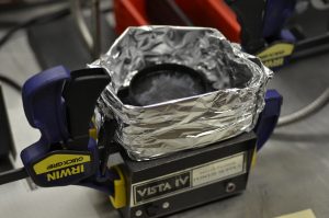
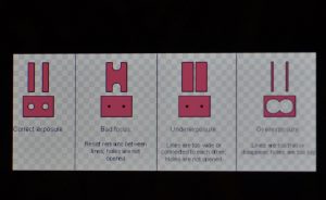
- Expose active area
- Develop 1:3 400k KOH:H20 puddle 1 min
- Water rinse (no solvent)
- Inspect wafer, if defect strip resist and retry
- Hard bake 15 min @ 125c hotplate
- Etch active area – 1-2% HF 15 min or until surface hydrophobic
- Water rinse
- Resist strip – Acetone or plasma ashing 100 watts RF 5 min @ 125mTorr O2
- IPA rinse
- Water rinse
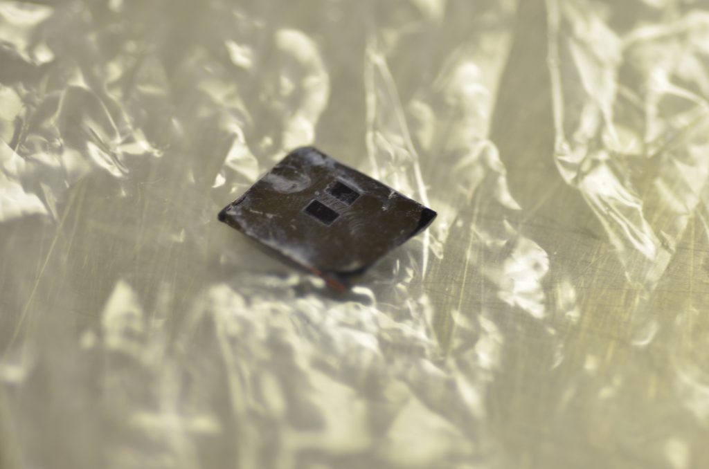
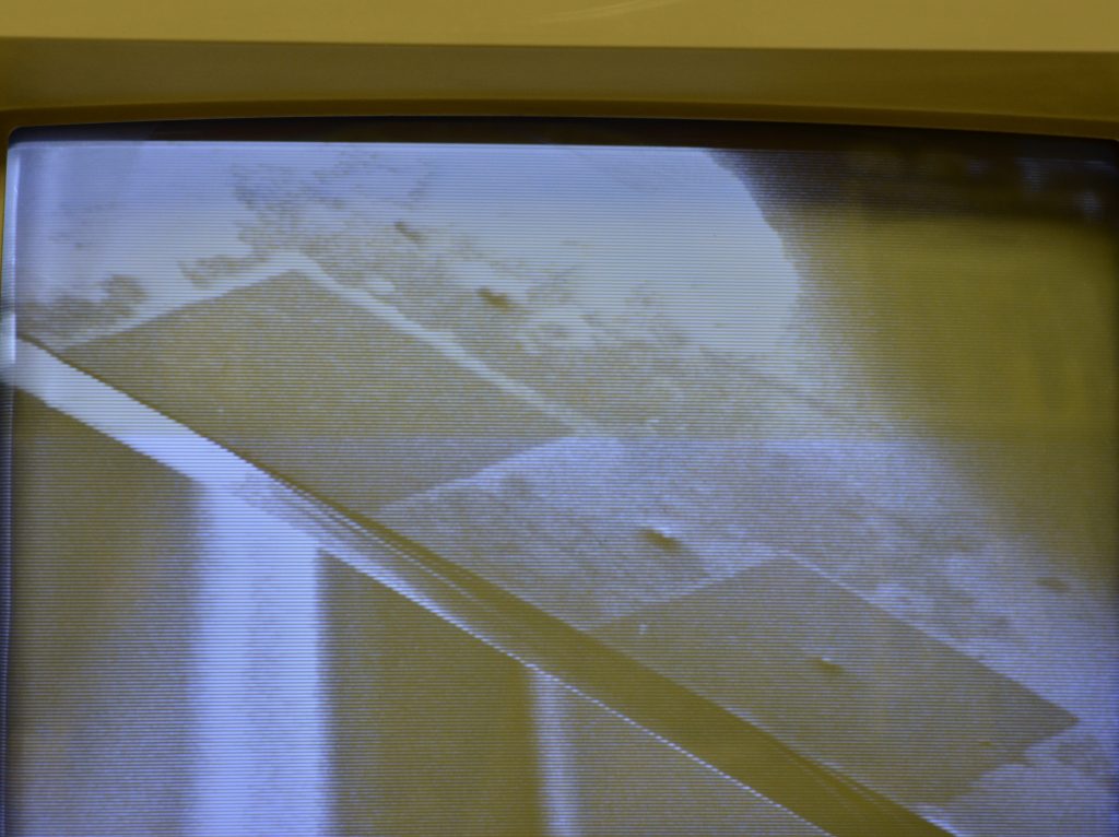
Tall particles can easily short out the thin gate oxide in these devices, as shown under my SEM. This poses an issue for making such devices in a garage; the gate oxides must be grown thicker to mitigate shorted devices which leads to a higher threshold voltage for the FET.



You might be able to solve your problem with tiny particles shorting gate and other defects by building some sort of big glove box with filtred air inside it where you whould have all equipment needed to make chips. That way you could have very clean enviroment without building a whole cleanroom. I think it whould be possible to do and probably not that expensive. I hope I helped. Also please can you tell me what is the heating element of your tube furnace made out of? Is it nichrome? And what is the wattage of your furnace? I am trying to make my own tube furnace from scratch and I am not sure how to pick the right resistive wire lenght. I whould love to try to make some basic diodes or even transistors too. Thanks.