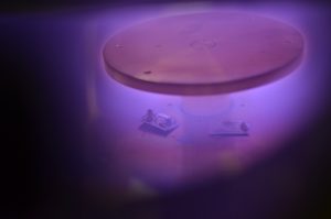
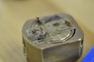
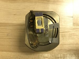
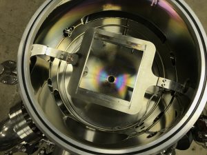
Thin films of copper were prepared on non-conductive samples to be observed under the Electron Microscope. This process is called DC Diode Sputtering and took place at just below 100mTorr and 2000v @ 150watts.

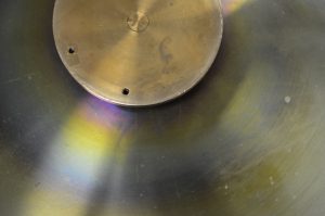
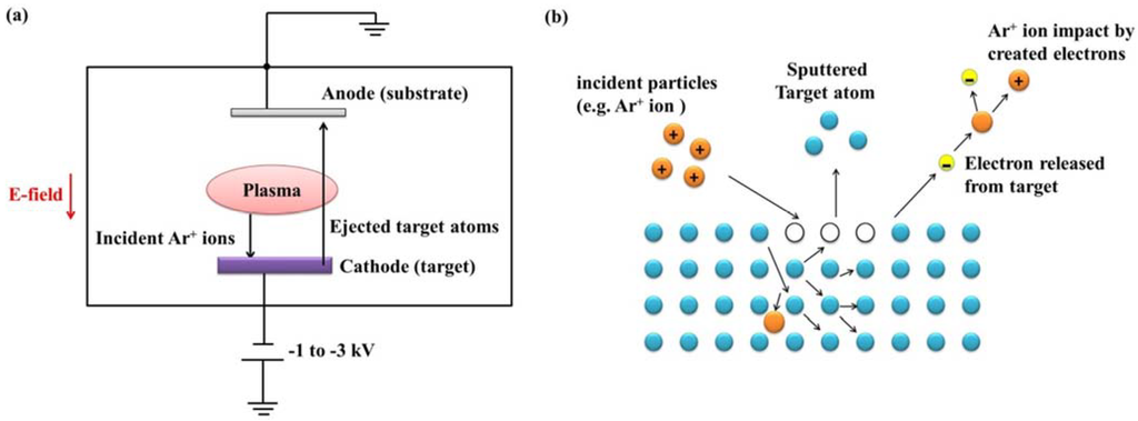
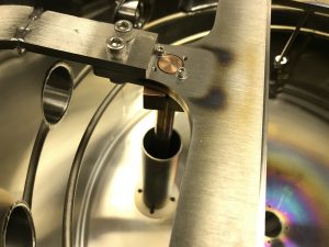
This same setup can be used at lower powers to plasma clean or etch the top layer surface of the sample for better images under the SEM. Oxygen (and sometimes a small amount of Nitrogen) is usually a much more effective gas for this cleaning than Argon and leads to less unwanted sputtering as well.
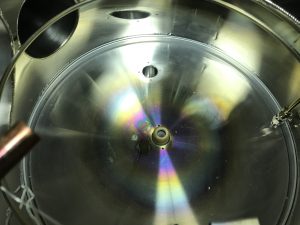
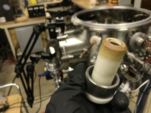
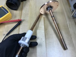
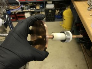
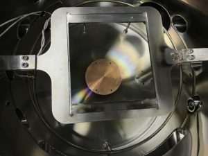
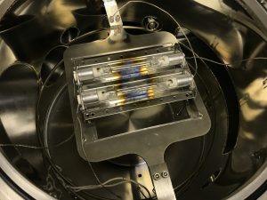
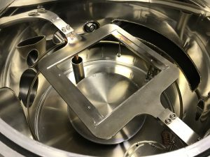
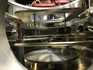
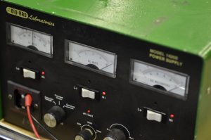
Sputtering system v2 was made to support DC and RF sputtering so I can make dielectric coatings as well and it supports larger target and substrate samples. An insulator will be constructed to mount the target holder to the main chamber walls so that RF can be used more effectively.
(Click on image to enlarge)
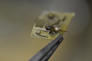
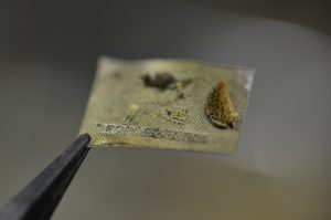
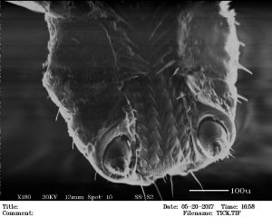
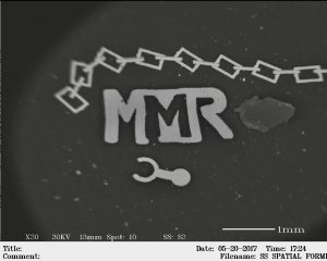
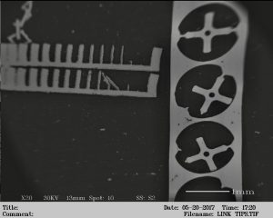
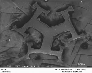
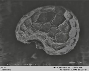
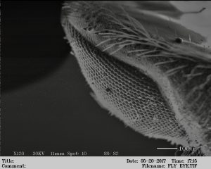
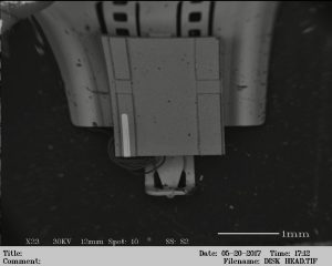
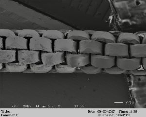
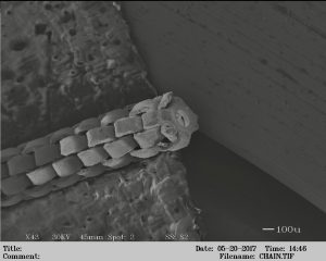
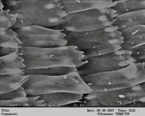
SEM Demo
do you believe you need to be able to see the plasma for any reason or if you had an opaque chamber it would be ok?