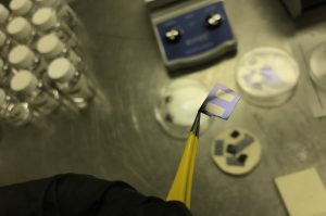
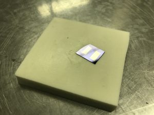
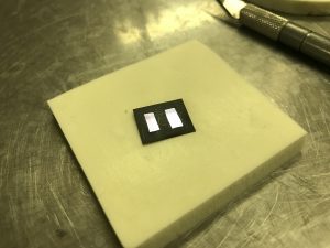
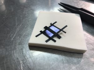
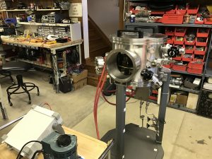
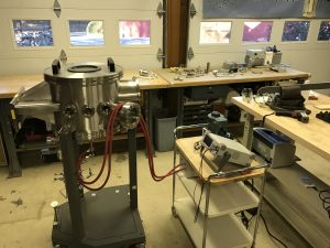
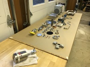
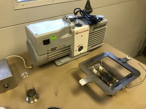
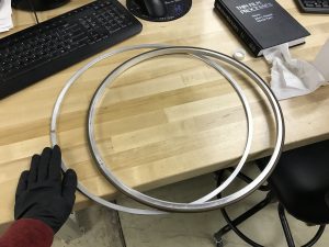
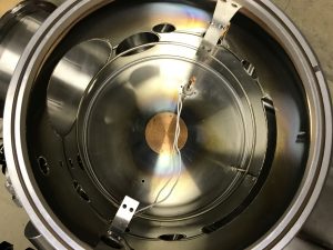
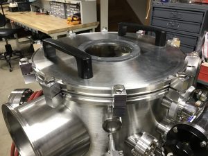
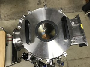
Rewound MOT for thermal evaporation – 800amps and new Lindberg 1″ tube furnace for diffusion
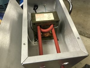
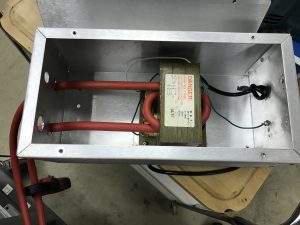
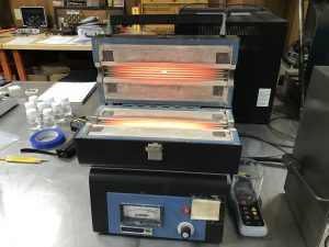
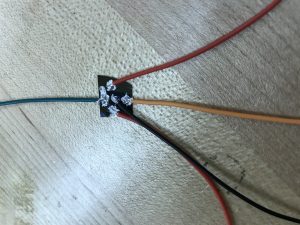
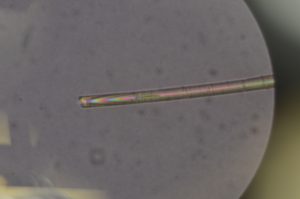
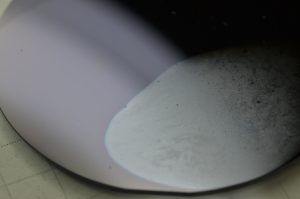
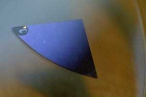
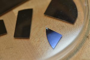
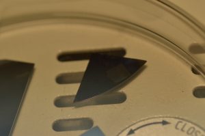
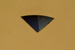
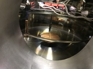
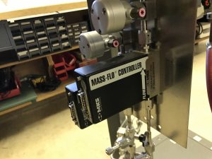
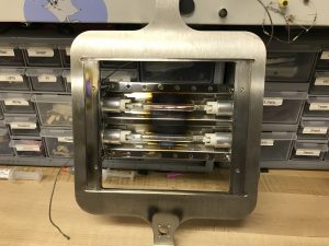
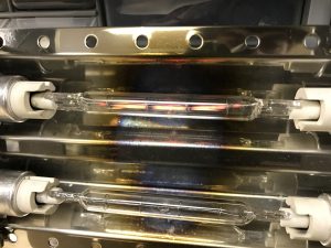
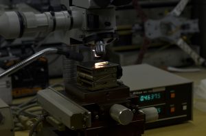
Rewound a microwave oven transformer using 1 gauge welding wire. Before saturation it puts out 1.8volts ish. I plan to use it to heat up a tungsten boat for thermal evaporation deposition. I may rewind it with slightly thinner wire so I can get more turns on the secondary and a little higher voltage. Last picture is a new/old Lindberg 1″ dia. tube furnace I got, goes up to 1400c which is crazy. I use it for diffusion of N type and P type dopants into my homemade semiconductors as well as thermal oxidation. I have a large nitrogen tank which allows me to create a nitrogen atmosphere in it during diffusion and when I want to facilitate SiO2 growth I pump steam through the furnace and turn the nitrogen flow off. I have a mass flow controller for the nitrogen but haven’t hooked it up yet.
Fabrication and Characterization of N-Channel Enhancement Mode Insulated Gate Field Effect Transistors
Update 4/25/18: First IC!
Update 8/27/17: Developing Patterning Process for Homemade Microelectronics
Update 7/30/17: Developing Metalization Process for Homemade Microelectronics
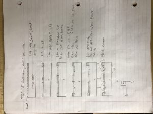
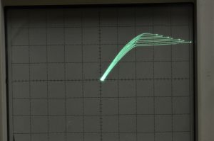
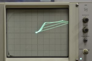
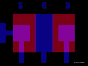
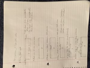
These are my first working transistors. Specifically, they are insulated gate enhancement mode n channel field effect transistors. I also made a depletion mode FET with a conducting channel and it worked even better than the enhancement mode ones. I drew out the steps I took to make this, they’re based on Jeri Ellsworth’s work but with a few main changes. It is very important that your dielectric overlap source and drain regions on the FET, otherwise no inversion layer can be formed and the FET cannot turn on. Only a small overlap is necessary and the larger it is, the more unwanted capacitance there is. This is not normally a consideration in actual production because inherent lateral diffusion takes care of the overlap but for these large hand made devices I found you have to get very lucky with your alignment if you don’t budget extra overlap.
A huge thanks to Jeri for making her videos about home chip fabrication which got me interested in these experiments in the first place.
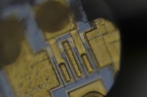
You can see in the center of the transistor there is a red region of silicon dioxide, this is the gate and the color indicates that it is roughly 750 angstroms thick. I would like to make the gate thinner so I can achieve lower threshold voltages, etc. but it is hard to make a truly insulating gate much thinner than that in a dirty environment because of pinholes and other impurities in the oxide layer.
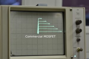
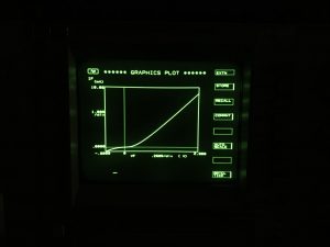
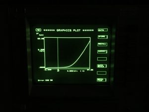
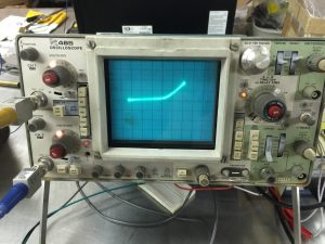
Diode characteristics are characterized with a semiconductor parameter analyzer
A brief introduction to semiconductor fabrication processes and terminology. It is not intended to be an in depth view of any single process, but rather an overview so that provides enough information for someone to get started with making diodes and transistors at home.
Tour of my home chip fab setup in early 2017. I’ve been accumulating this equipment since October of 2016.
Step by step FET fabrication
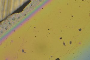
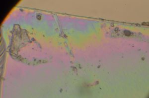
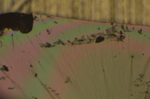
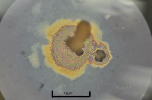
Oxide and Spin on Diffusant Thin Film Interference Patterns on Wafers
As of now, I am doing all of my doping with spin on diffusants. Some of which are solutions of Phosphoric/boric acid in alcohol/water that I prepared myself. I find it hard to control the dopant concentration and therefore bandgap of devices so my solar cells often have a bandgap too high or too low. I thought using an actual spin on dopant would help, so I bought some P509 phosphorus glass from Filmtronics and it works about the same as the solutions I made, except it spins on much nicer.
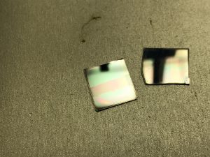
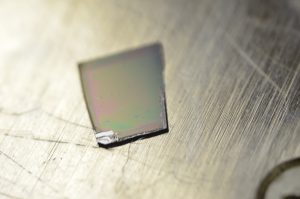
The colors you are seeing are contamination and nonuniformity in the thin film interference patterns caused by this thin glass layer after pre deposition of the spin on diffusants.
Continue reading Oxide and Spin on Diffusant Thin Film Interference Patterns on Wafers
Silicon Wafer Pics – Thermal Oxidation
Blue color indicates roughly 500nm SiO2 thickness. It took about 2.5hours to grow @ 1200c in a pottery kiln style furnace with steam being pumped into it. Picture above on the left shows moisture on cooling wafer. Picture on the right shows unpolished backside of the wafer. Notice the nonuniformity in the growth thickness caused by unequal heating. This is because I don’t have a quartz boat to hold the wafers so I place them face up in the furnace. Continue reading Silicon Wafer Pics – Thermal Oxidation
DIY PN Junction Diode Fabrication
Interesting Read – The Lost Knowledge of Point Contact Field Effect Devices (Fieldistor)
High Vacuum Chamber and Parts for PVD and Plasma Etching
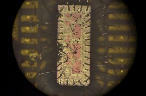
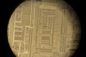
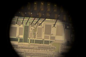
Medtronics Pacemaker Silicon IC Dies Under Microscope
Homemade Photovoltaics – DIY Silicon PN Junction Solar Cell Testing
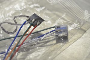
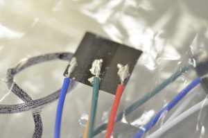
Testing of homemade solar cells/PN junction diodes. Some of them output up to .25v open circuit and a few hundred microamps at short. This varies widely because of changes in dopant concentration and wafer size. The higher dopant concentration makes a lower bandgap. Most of these devices have a band gap that is too low to be most efficient for a solar cell. Optimally I would want about 1.4ev. As dopant concentration increases, the wave functions that describe the electrons in both valence and conduction bands start to converge and overlap so the bandgap basically gets broken and the solar cells preform very poorly. I estimate about 1% efficiency on these cells, most likely less.
