Homemade Memristors
Memristors are interesting devices first posed by Leon Chua in 1971 as the 4th basic circuit element, after the resistor, capacitor, and inductor. It would theoretically satisfy a relationship between charge and flux, and in simple terms is a 2-terminal device whose instantaneous resistance depends on the device’s electrical past (total charge or current that has flowed through the device). The possibility for existence of a memristor in our universe is highly debated and claims of “discovering” the missing memristor were circulated by HP Labs in 2008. The resistance-memory effect they noted was met with huge amounts of press and recognition, but in reality it was first noted in the late 1960s in similar materials and was not valid under the original mathematical definitions for a memristor. Since then, the definition and requirements for a memristor have been relaxed by some and even Leon Chua himself has recognized HP’s memristor. As with most politics and similar situations in academia, you should read about this on your own and come to your own conclusions, but it is safest to describe such devices with a resistance-memory as “memristive devices” or “memristive systems”, because while they may not adhere to the original definition of a memristor, they are still worth exploring and have proved to be useful for machine learning and artificial neuron applications. Interestingly, an ideal memristor fits as a perfect electrical model for Axons/synapses.
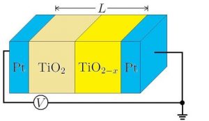
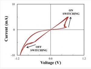
Most of these memristors are made with some metal oxide stack with top and bottom electrodes and rely on the electrical current moving oxygen vacancies within the metal oxide to create a sort of hysteresis in resistivity. The results in a unique pinched-figure-eight hysteresis type IV curve whose loop area decreases with increasing frequency:

Basic memristive devices can also be made easily at home out of Copper Sulfates, as described here and here. Of course, it is advantageous for lots of reasons to be able to manufacture these on a parallelized, industry standard CMOS-type fab process, where thousands of these devices can be made at once using photolithography.
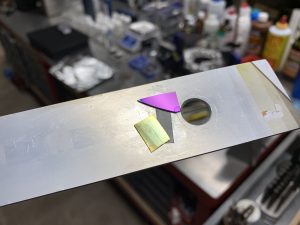
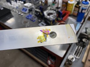
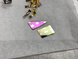
About 2 years ago when I was setting up my sputtering chamber, none of the coatings were conductive. This was frustrating but eventually I figured out the films were metal oxides, not pure conductive metal coatings, due to too much Oxygen being present during the sputtering. Recently, I read that memristive devices can be made out of materials such as Titanium and Copper oxides, so I dug out some old failed sputtering attempts of these materials, put them back in a chamber to deposit a top Copper electrode, and measured their IV characteristics.
Both Titanium and Copper oxide based devices worked as memristive systems and showed similar characteristics. The bottom electrode in both cases was doped Silicon which causes the devices to be slightly rectifying (asymmetry in curve) and highly sensitive to light (built-in PN junction) but they still show a resistance-memory hysteresis effect. In the future, more devices will be built on insulating substrates and should yield much better results. Rectifying memristors made on Si substrates have applications in high density 3D array stacks, even though they deviate highly from an “ideal” memristor.
Figure (a) above shows a typical curve from one of my devices and figure (b) shows a curve from a paper published studying similar metal oxide-based memristors. Scale on fig. (a) is 100uA and 5V per division.
Here, differences in slope (1 / resistance) for the on (blue) and off (red) regions can clearly be seen, as well as the switching region (yellow).
As previously mentioned, these devices are highly light-sensitive due to the doped Si substrate and a have very strange response:
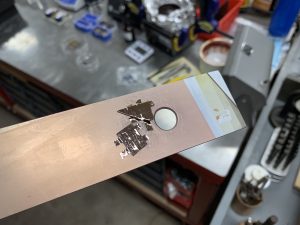
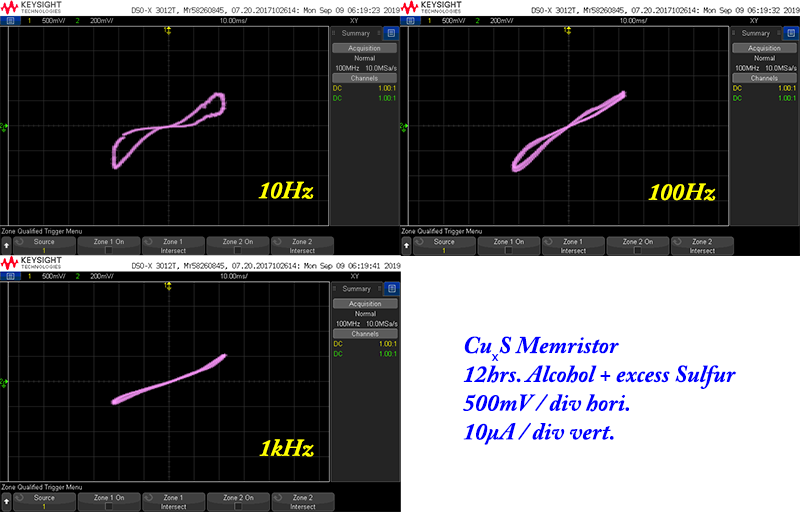
After these first encouraging results, I made Copper Sulfide based devices that actually exhibit more ideal characteristics and can be made for a few dollars. Excess pure Sulfur powder from Amazon is dissolved in Ethanol or Isopropyl alcohol and a bare Copper PCB was placed in solution for 12 hours. The experiment was in a closed vessel to avoid evaporation and a black CuₓSᵧ film was noted. Then, the device was washed in alcohol for 3 hours to remove any residual Sulfur particles before being probed with a function generator and oscilloscope wired as a curve tracer.
Homemade CuₓSᵧ memristors:
A nice figure-eight is seen to pass through the origin and have a loop area which is decreasing with increasing frequency, as expected by the equations that govern a memristor (time integral of charge or current).




Look into radioactive isotopes. They have similar effects shown when creating memories in micro organisms. Heard your going to Cambridge? Have Fun.
can you provide a link or paper about this phenomena? also, I’m to carnegie mellon which is going well thank you.
Hello, can you provide more details on how to make these at home? Great work, thank you!
you can work on multi stage memristive device based on stress induce film on pizo electric substrate
They’re not technically memristors, but the resistive RAM used in Intel’s 3D Xpoint and Micron’s QuantX memory (purchasable on Amazon as Optane memory with RAM speed in SSD sizes!) has many of the same characteristics and basically is the modern memristor in my view.
The basic idea for ReRAM is that you cause chemical migration of atoms/species to make a conductive path between electrodes. This stores memory because the path stays there after you switch off the voltage. The special part is choosing those species to move fast enough to be useful for computers. It would be interesting to see if you could manufacture some ReRAM devices (chacogenide, or even oxide-based ones) and then image the conducting paths using your SEM and EDS!
Side topic: I think you might have a lot of fun making a scanning tunneling microscope (STM). A lot of your old work has been on the micron scale, but you can quite easily bring it down to the atomic/angstrom/nanometer scale with an STM. I saw some simple DIY designs before, but have not been very impressed since they only look at graphite. I think there is quite a bit that can be done with garage-style engineering on STM if someone took the time.
All in all, very impressed with your work. I can’t imagine how supportive your family must be personally and financially, getting a garage with custom piping, electronics, a full electron microscope, etc. is no small feat! No way I could afford any of that in my studio apartment haha. Keep at it Mr. Zeloof!